Download
1 / 21
220 likes | 363 Views
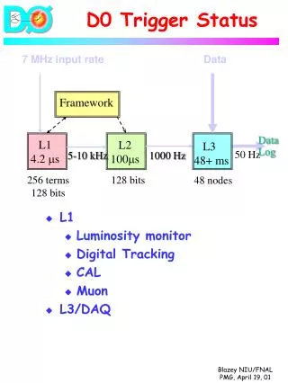
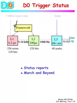
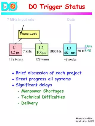
The Trigger Prototype Board Status. On behalf of trigger group D. Nicolò F. Morsani S. Galeotti M. Grassi. Marco Grassi INFN - Pisa. PMT. FADC. FPGA. 16. Clock Sync Trigger Start. 48. 4. 48. 48. 4. VME. Sync. LVDS Trans. LVDS Trans. Hardware: board Type 1. VME 6U

E N D
The Trigger Prototype Board Status On behalf of trigger group D. Nicolò F. Morsani S. Galeotti M. Grassi Marco Grassi INFN - Pisa
PMT FADC FPGA 16 Clock Sync Trigger Start 48 4 48 48 4 VME Sync LVDS Trans LVDS Trans Hardware: board Type 1 • VME 6U • A-to-D Conversion • FADC with differential inputs bandwidth limited • Trigger • LXe calorimeter • timing counters • No use for the tracking chambers • I/O • 16 PMT signals • 2 LVDS transmitters • 4 in control signals 16 x 10 Control FPGA Type 2 boards
LVDS Rec 10 x 18 FPGA Clock Sync Trigger Start Out 48 48 48 4 4 18 3 3 18 VME Sync LVDS Trans LVDS Trans Hardware: board Type 2 • VME 9U • Matched with the Type 1 boards • I/O • 10 LVDS receivers • 2 LVDS transmitters • 4 in control signals • 3 out signals Type 1 10 x 48 Trigger Sync Start Control FPGA to next Type 2
. . . . . . . . . 12 or 6 boards 20 boards 10 boards Type1 Type1 Type1 Type1 Type1 Type1 Type1 Type1 Type1 4 4 4 16 16 16 Type2 Type2 Type2 Type2 Type2 Type2 4 x 48 4 x 48 10 x 48 20 x 48 12 x 48 Hardware: system structure 2 boards LXe inner face (312 PMT) LXe lateral faces (208 PMT) (120x2 PMT) (40x2 PMT) 1 board 1 board 2 x 48 2 or 1 boards Timing counters (160 PMT) or (80 PMT) 2 VME 6U 1 VME 9U
Present status • Prototype board: Type0 • ModifiedType1: • Check of the connectivity with the Type2 • Study the FADC coupling • Verify the chosen algorithms • Selected components (all delivered) • MainFPGAXCV812E-8-FG900 and XCV18V04 config. ROM • Interface and control CPLDXC95288XL-FG256 • ADCAD9218(dual 10 bits 100 MHz) • Clock distributionCY7B993V(DLL multi-phase clock buffer) • LVDS serializerDS90CR483 / 484(48 bits - 100 MHz - 5.1 Gbits/s) • LVDS connectors3M Mini-D-Ribbon • Analog input by 3M coaxial connectors • Control and debug signals in LVDS standard • FPGA design completed • FPGA designand simulation completed (runs at 100 MHz) • VHDL parameterization is ready
LVDS Rec PMT FADC FPGA 16 Clock Sync Trigger Start Out 4 4 16 16 48 4 48 3 48 4 Sync 2 boards Type0 Type0 Trigger Start LVDS Trans Prototype board : Type 0 • VME 6U • A-to-D Conversion • Trigger • I/O • 16 PMT signals • 2 LVDS transmitters • 4 in/2 out control signals • Complete system test Analog receivers 16 x 10 Control CPLD Sync Trigger Start Spare in/out VME
The Analog input stage AD8138 • BW limitation • Unipolar or bipolar inputs • Variable gain • Pedestal adjust
Board Design completed • Implementation by means ofCADENCE • Schematic simulation completed • Components footprints checked • Board routing ready • 10 layers 4 GND Power 6 signals • DC/DC converters • A32 mode • Block transfer • Board production • PCB producer contacted: ready for a production offer • Delivery: end of July • Test: September
DRS Chip • Prototype received Nov. 02 • Tests Dec. 02 – April 03 • Digital part works perfectly • Analog parts requires redesign • DLL and VME board built by Siena
Test results fsamp[GHz] vs. Vdd[V] fsamp[GHz] vs. Vcontrol[V] fsamp[GHz] vs. T[deg. C]
Running Domino Wave Denable Dtap Jitter after 32 turns: ~1ns 32 Domino cycles @ 320ns Readout Shift Register SR_CLK SR_RESET SRIN SROUT #768
In Vspeed Phase Comparator DLL Ext. quartz clock DLL Design R. Paoletti, N. Turini, INFN • DLL works with jitter of 200 ps RMS • Siena (N. Turini, R. Paoletti, MAGIC) designs VME board
DRS Readout Input pulse Digitized output pulse 5ns risetime 8ns risetime
Problems in analog part source Capacitances: Gate-Bulk: 10.6 fF Source-Bulk: 13.5 fF Drain-Bulk: 2.4 fF gate drain PHI Csamp PHI Bus Bus capacitance too high (110pF)
DRS Redesign • Reduce bus-bulk capacitance by 6x • Reduce bus-bus capacitance • Use current-mode readout R I Vin Vout read write . . . G. Varner, Univ. of Hawaii: STRAW2 chip C
Plans • UMC 0.25mm technology • Next Submission Oct. 20th • Production time ~9 weeks • VME board design in parallel (Siena) • Rectangle 5 x 5 mm2 • Reduce minimum sampling speed to 500 MHz (for DC) • Daisy chain mode for N x 1024 bins • Dual-channel for deadtimeless operation • 4 chn. Q mode + 4 chn. I mode • Production run spring 2004
DRS options Input Input Readout Domino Wave Dual-channel mode Daisy-chain mode
DRS (DAQ) 2002 2003 2004 2005 1st Prototype Tests 2nd Prototype Boards & Chip Test Design Manufactoring Assembly Test Milestone
DAQ System 800 + 160 area ~7m to trigger (~20m) Trigger PMT Active Splitter monitor 10 VME crates ~2m optical fiber (~20m) DRS Board (16chn) Front-End PCs Rack – PC (Linux) SIS 3100 Rack – PC (Linux) Rack – PC (Linux) 1920 ~7m Rack – PC (Linux) DRS Board (16chn) DC Pre-Amp Rack – PC (Linux) Gigabit Ethernet Rack – PC (Linux) Rack – PC (Linux) Rack – PC (Linux) Raw data: 2880 channels 100 Hz 50% / 10% / 10% occupancy 2kB / waveform -> 5 x 25 MB/sec. Rack – PC (Linux) Rack – PC (Linux) Fitted data: 10 Hz waveform data -> 1.2 MB/sec 90 Hz ADC / TDC data -> 0.9 MB/sec Rack – PC (Linux) On-line farm storage
Waveform analysis Original Waveform • Zero suppression in FPGA • Single hit • ADC/TDC derived in FPGA • Multiple hit • Waveform compressed in FPGA (2x12 bit -> 3 Byte) • Waveform fitted / compressed in PC cluster • Store ADC/TDC only for “calibration” events • Store (lossless) compressed waveforms for MEG candidates Region for pedestal evaluation T integration area Difference Of Samples Threshold in DOS ADC2/TDC2 ADC1/TDC1
ROOT for online analysis • ROOT becomes more stable and is now widely used • “Online extensions” are underway (life display of histos and N-tuples) • Propose to use ROOT for online monitoring and single event display, CARROT for Web display • For offline analysis, keep possibility to use ROOT or PAW ROOT GUI offline analysis ROOT *.root ROOT Analyzer FE offline analysis HBOOK *.rz PAW *.mid online offline