Download
1 / 15
160 likes | 371 Views
彰師大 積體電路設計研究所. A 0.6V ULTRA LOW VOLTAGE OPERATIONAL AMPLIFIER. 指導教授:林志明 所長 指導學生:賴信吉 Email : s94662005@mail.ncue.edu.tw. Y. Tang and R. L. Geiger, “ A 0.6V ULTRA LOW VOLTAGE OPERATIONAL AMPLIFIER , ” IEEE International Symposium on Circuits and Systems, Phoenix, May 2002 .

E N D
彰師大 積體電路設計研究所 A 0.6V ULTRA LOW VOLTAGE OPERATIONAL AMPLIFIER 指導教授:林志明 所長 指導學生:賴信吉 Email:s94662005@mail.ncue.edu.tw
Y. Tang and R. L. Geiger, “A 0.6V ULTRA LOW VOLTAGE OPERATIONAL AMPLIFIER,” IEEE International Symposium on Circuits and Systems, Phoenix, May 2002 . Department of Electrical and Computer Engineering Iowa State University, Ames, IA 50011, U.S.A
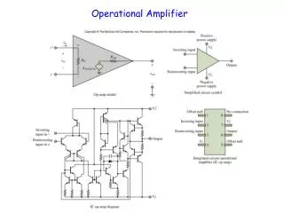
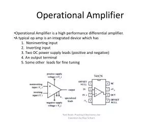
Outline • Introduction • Threshold voltage tuning • Design of the low-voltage OP AMP and it’s supporting circuits • Simulation results and comparison • Conclusion
Introduction • Low-voltage circuit design. • Voltage sources are added in series with the gates of the MOS transistors. • A standard 3.3V 0.35μ CMOS process without modifications. • Around threshold voltage level • 20% power consumption of 3.3V counterpart.
Threshold voltage tuning • Supply voltage limitation.→ Vth, VDSAT. • Threshold voltage around 0.7V. • The minimum supply voltage has been around 1.5V.
§ The basic concept of this low voltage technique is very simple.§ It will have the same gm and go if biased at the same drain current level.
Design of the low-voltage OP AMP and it’s supporting circuits
NMOS • φ1 and φ2 are non-overlapping clocks. • CMOS Rin ↑, switch leakage current ↓, soφ1 and φ2 can be low to reduce noise injection.
0.6V 0.5MHz range 0 1 Frequency divider:D flip-flop, 64:1.
Bias voltage generator (simple self-biased circuit under 0.6V) • Roughly 0.2V below the threshold voltage. • Provide enough current so that during the charging of C1.
Issue…… • N-well CMOS process. • Switches → NMOSbodies →ground • Leakage < 1μA
Simulation results and comparison • To compare the performance of the low-voltage Op Amp (3.3V power supply, Vtn=0.55V, Vtp=0.6V, 0.35 μm CMOS process. )
Conclusion Simulation results show….. • It maintains the key small signal parameters. • Low voltage circuit exhibits a major decrease in power dissipation.