Download
1 / 15
150 likes | 159 Views
Prototype of the SVD Finesse Transmitter Board (FTB) (Sender Part for HSD Link). The Prototype of the SVD FTB Recent Status f or PXD+SVD combined DAQ session on Wednesday at 3rd Belle II PXD/SVD Workshop and 12th International Workshop on DEPFET Detectors and Applications

E N D
Prototype of the SVD Finesse Transmitter Board (FTB) (Sender Part for HSD Link) The Prototype of the SVD FTB Recent Status for PXD+SVD combined DAQ session on Wednesday at 3rd Belle II PXD/SVD Workshop and 12th International Workshop on DEPFET Detectors and Applications in Wetzlar, Germany 4-6 February 2013 06.02.2013 wacek ostrowicz 14 slides
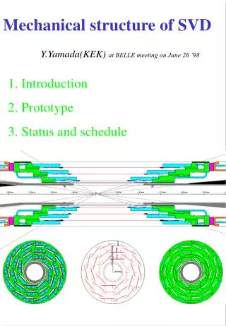
Prototype of the SVD Finesse Transmitter Board (FTB) (Sender Part for HSD Link) I. SVD Electronics - general view II. Status of Hardware III. Status of Firmware IV. Schedule V. Summary 06.02.2013 wacek ostrowicz 1/14
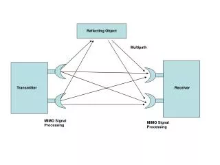
Giessen Box COPPER#48 SVD tracker opt FRB opt opt #1 #48 FADC#48 FTB#48 FADC#1 COPPER#1 RJ45 opt FRB opt opt opt RJ45 FTB#1 RJ45 opt opt opt RJ45 FADC-CONTROLLER (FADCctlr) RJ45 Prototype of the SVD Finesse Transmitter Board (FTB) (Sender Part for HSD Link) SVD Electronics - general view PIXEL F E E l e c t r o n i c s … DAQ … SVD electronics RJ45 JTAG #48 TTD RJ45 … FTSW RJ45 JTAG #1 TTD RJ45 RJ45 TTD #49 06.02.2013 wacek ostrowicz 2/14
Prototype of the SVD Finesse Transmitter Board (FTB) (Sender Part for HSD Link) II. Status of Hardware 1. PCB Design version2 2. List of changes 3. TTD and GTP Clock distribution. Clock Domains 06.02.2013 wacek ostrowicz 3/14
Prototype of the SVD Finesse Transmitter Board (FTB) (Sender Part for HSD Link) FTB Prototype version2 8 4 6 5 3 2 7 1 8 06.02.2013 wacek ostrowicz 4/14
Prototype of the SVD Finesse Transmitter Board (FTB) (Sender Part for HSD Link) List of changes 1. LVDS outputs for TTD moved to Bank2 2. One Oscillator 127MHz + DS25CP152 chip. 3. TTD Clk connected to GTP RefClk pins. 4. 32MHz Oscillator on board 5. Third OptoLink 6. Different drivers 7. Changed pin-out 8. XC6SLX75T -> XC6SLX100T Logic Cells: 74,637 -> 101,261 Slices: 11,662 -> 15,822 Max Distributed RAM (Kb): 692 -> 976 Block RAM Blocks [Max (Kb)]: 3,096 -> 4,824 Price: $140 -> $176 9. Module equipped with Front Plate -> no backplane between FADC and FTB 06.02.2013 wacek ostrowicz 5/14
Prototype of the SVD Finesse Transmitter Board (FTB) (Sender Part for HSD Link) TTD and GTP Clock distribution. Clock Domains. FPGA ENABLE SELECT[1:0] GTP X0Y0 Oscillator 127MHz REFCLK0 REFCLK1 MUXDS25CP152 Diff Input 127MHz TTD core from/to TTD RJ 45 Gclk FPGA FTB DATA Opto Transceiver GTP Transceiver Main Part of FPGA DCLK FADC GTP Clk 127MHz FADCRDY MUX 32 MHz FPGA init ADC&FTB READY TTD core 127MHz from TTD & FTBRDY 06.02.2013 wacek ostrowicz 6/14
Prototype of the SVD Finesse Transmitter Board (FTB) (Sender Part for HSD Link) III. Status of Firmware a) main goals of FTB 1. Receive DATA from FADC 2. Input DATA CRC checking 3. Receive EventNumber and Trigger from DAQ and calculate FTB_EventNumber 4. Checking and reporting differences with Event Number coming from DAQ, FADC and FTB 5. Inserting HEADER and TRAILER 6. Output DATA CRC calculation. 7. Preparing DATA and control signals for BELLE2 Universal Core. 06.02.2013 wacek ostrowicz 7/14
Prototype of the SVD Finesse Transmitter Board (FTB) (Sender Part for HSD Link) main goals of FTB cont… 06.02.2013 wacek ostrowicz 8/14
Prototype of the SVD Finesse Transmitter Board (FTB) (Sender Part for HSD Link) III. Status of Firmware b) FTB Interfaces 1. Interface between FTB and FADC 2. Interface between FTB coreand Belle2Link core 3. Interface between FTB coreand PXD core 4. Interface between FTB coreand TTD core RJ45 FTSW (JTAG) 3 PXDcore Opto Transceiver PXD 1 Main Part of FPGA FADC 2 B2Lcore Opto Transceiver B2Link 4 TTD core RJ45 FTSW (TTD) FPGA FTB 06.02.2013 wacek ostrowicz 9/14
Prototype of the SVD Finesse Transmitter Board (FTB) (Sender Part for HSD Link) Universal part IDENTICAL for ALL subdetectors Part dependent on subdetector DATA format -> FF[31:0] -> FWENB -> FWCLK <- FFUL <- NWFF COPPER FINESSE <> LD[7:0] <- LA[6:0] <- LRW <- CSB <- TAG[7:0] <- TRG <- CLK <- IRSTB -> BSYB -> FRSTB 06.02.2010 wacek ostrowicz 10/14
Prototype of the SVD Finesse Transmitter Board (FTB) (Sender Part for HSD Link) III. Status of Firmwareb) interface to OptoLinks for DATA - proposal DATA(31:0) Core for PXD Link BoE FIFO for PXD Link Read FIFO EoE OpTr To PXD FIFO empty Output FIFO FIFO full SVD Logic write FIFO DCLK GTP CLK FIFO full MAIN FIFO for HSD Link >120kB Unified core for HSD Link DCLK Read FIFO OpTr HSD Link Event Rdy FIFO empty Read FIFO end of Event DCLK GTP CLK write FIFO HSD Link side requires to collect the whole Event before sending out Logic FIFO full 06.02.2013 wacek ostrowicz 11/14
Prototype of the SVD Finesse Transmitter Board (FTB) (Sender Part for HSD Link) III. Status of Firmware c) what has to be done 1. Interface between FTB coreand Belle2Link core 2. Interface between FTB coreand TTD core 3. Remote FPGA configuration 4. Interface between FTB core and on board serial PROM No significant progress since last B2GM meeting 06.02.2013 wacek ostrowicz 12/14
Prototype of the SVD Finesse Transmitter Board (FTB) (Sender Part for HSD Link) IV. Schedule Production of 5 modules of the FTB module ver2. January February March April PCB design is ready Production of the PCB Ordering the parts Mounting modules Basic tests of the modules Distribution 1 module to KEK 1 module to PXD 2 modules remain in Krakow (will be used for DESY test) 1 spare module to ??? 06.02.2013 wacek ostrowicz 13/14
Prototype of the SVD Finesse Transmitter Board (FTB) (Sender Part for HSD Link) IV. Summary The most important and urgent goals: 1. Start the PCB production. 2. Agree on the Interface between Belle2Link core and FTB core 3. Start the Modules production 3. Agree on theInterface between TTD core and FTB core 4. Finish full FTB firmware. Thank you 06.02.2013 wacek ostrowicz 14/14