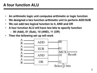
Download

1 / 22
240 likes | 1.01k Views
4bit-ALU (Arithmetic Logic Unit). Lam Nguyen Vinh Nguyen The Dao Advisor: Dr. David Parent Date: 12/05/05. Agenda. 1. Abstract 2. Introduction - Why? - Background Information 3. Project Summary - Schematic - Layout

E N D
4bit-ALU(Arithmetic Logic Unit) Lam Nguyen Vinh Nguyen The Dao Advisor: Dr. David Parent Date: 12/05/05
Agenda 1. Abstract 2. Introduction - Why? - Background Information 3. Project Summary - Schematic - Layout - LVS report -Longest Path Calculations -Lessons Learned 4. Summary 5. Acknowledgements
Abstract Our designed project 4-ALU performs the following functions: • AND • OR • XOR • ADDER Area = 390µm×590µm =0.23µ m2
Introduction • ALU is a basic fundamental unit of any computing system. • Understanding how an ALU is designed and how it works is a benefit to build any advanced logic circuits. • Using this experience, we can have a basic to design a more complex IC.
Project Details • Create Schematics and layouts for And, Or, Xor, Adder, flip-flop, and Mux in the Cadence tool. • Test the schematics by using test bench. • Create Schematic and layout for 1 bit ALU • Run DRC, extract and LVS for 1 bit ALU. • Connect Cout of the first bit to Cin of the second bit and continue to have 4 bit ALU. • Run the DRC, extracted LVS and simulation to check the final design.
1bit-ALU Logic Logic DFF DFF The design uses the concept of parallel operations.
4-to-1 Mux ALU handles two inputs of 4 bits each to produce a required output based on the output selection
4-1 Mux Wp = 9µ Wn = 4.5µ
4-1Mux Test Bench Time delay: τ = 0.5ns
1-bit Adder Wp = 7.8µ Wn = 9µ
4-bit Full Adder Time delay τ = 1.5ns
DFF Test Bench Time delay τ = 1.2ns
Simulation Select S0 =1 and S1=1 to have the longest path
Lessons Learned • Using Cadence tool • Designing an integrated circuit to met a specification. • Fixing errors from LVS report and extracted schematic file. • Using a same height for each layout cell to reduce the area.
Summary • Our designed 4-bit ALU can operate for the following operations: And, Or, Xor, Add • Our project has 372 transistors and 20 terminals. • The delay propagation is 5ns. • Area = 390µm×590µm =0.23µ m2
Acknowledgment • Thanks to professor David Parent for teaching and helping us throughout this project. • Thanks to Cadence Design Systems for VLSI Lab.