Download
1 / 5
300 likes | 1.37k Views
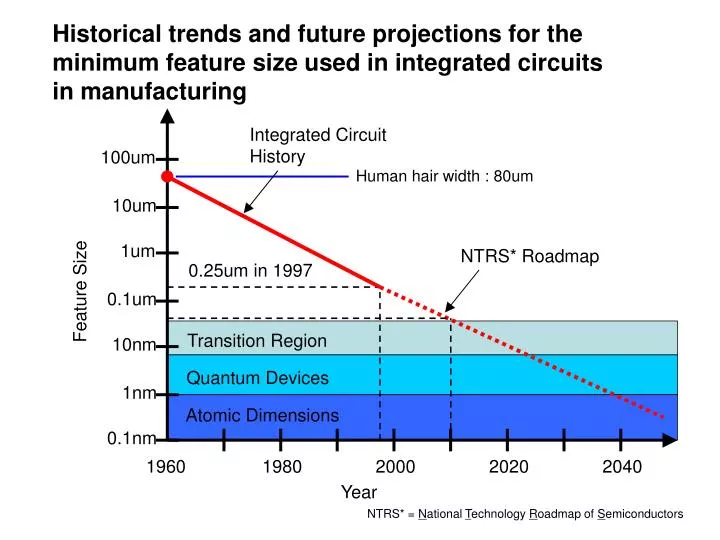
Integrated Circuit History. 100um. Human hair width : 80um. 10um. 1um. NTRS* Roadmap. 0.25um in 1997. Feature Size. 0.1um. Transition Region. 10nm. Quantum Devices. 1nm. Atomic Dimensions. 0.1nm. 1960. 1980. 2000. 2020. 2040. Year.

E N D
Integrated Circuit History 100um Human hair width : 80um 10um 1um NTRS* Roadmap 0.25um in 1997 Feature Size 0.1um Transition Region 10nm Quantum Devices 1nm Atomic Dimensions 0.1nm 1960 1980 2000 2020 2040 Year Historical trends and future projections for the minimum feature size used in integrated circuits in manufacturing NTRS* = National Technology Roadmap of Semiconductors
Year of first DRAM shipment 1997 1999 2003 2006 2009 2012 Minimum Feature Size 250nm 180nm 130nm 100nm 70nm 50nm DRAM Bits/Chip 256M 1G 4G 16G 64G 256G DRAM Chip Size (mm2) 280 400 560 790 1120 1580 Microprocessor Transistor/Chip 11M 21M 76M 200M 520M 1.40B Maximum Wiring Levels 6 6-7 7 7-8 8-9 9 Minimum Mask Count 22 22-24 24 24-26 26-28 28 Minimum Supply Voltage (volts) 1.8-2.5 1.5-1.8 1.2-1.5 0.9-1.2 0.6-0.9 0.5-0.6 Future projections for silicon technology taken from SIA NTRS
Basic process Light Photoresist Mask Deposition Film Substrate Film Deposition Photoresist application Exposure Development Etching Resist removal
Input Output Input Output CMOS Inverter What is CMOS ? W TiSi2 TiSi2 Ti TiSi2 P+ P+ N+ N+ P- P- N- N- N-Well P-Well P PMOS NMOS
L’ t’ox W’ 0.262nm 0.162nm Why needs Scaling? L tox W L=30nm, tox=1nm @IEDM2002 Toshiba, Sony • (1) Ids ∝ W/L x C x (Vg-Vth)2 • High Current drive • (a) Low Power (b) High Speed (2)Small Chip Area Low Cost, High Yield Silicon Oxygen particle Chip Size 1/2 Yield : ¾=75% Chip Failure