Download
1 / 37
370 likes | 404 Views
Explore the intricate process of making Micro-Electro-Mechanical Systems (MEMS) devices, utilizing materials such as semiconductors like silicon, metals for electrical contacts, and polymers as sacrificial layers. Dive into planar technology and micro-machining methods like wet and dry etching. Learn about MEMS fabrication steps, from photolithography to etching, and the history of MEMS development. Gain insights into materials used in MEMS, including semiconductors, metals, and polymers. Discover the MEMS process sequence and the importance of oxidation of silicon in MEMS device manufacturing.

E N D
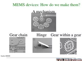
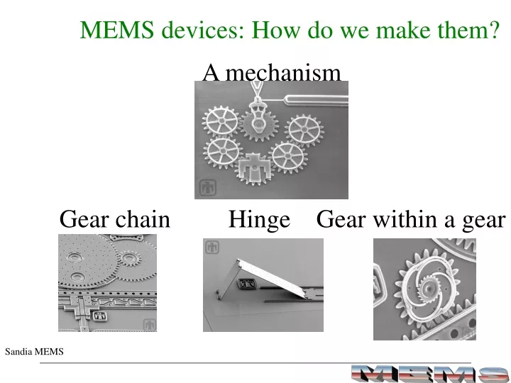
MEMS devices: How do we make them? A mechanism Gear chain Hinge Gear within a gear Sandia MEMS
Basic MEMS materials Silicon and its derivatives, mostly • Micro-electronics heritage • Si is a good semiconductor, properties can be tuned • Si oxide is very robust • Si nitride is a good electrical insulator
Materials in MEMS Dominant: SEMICONDUCTORS (Silicon centric) MEMS technology borrows heavily from the Si micro-electronics industry The fabrication of MEMS devices relies on the processing of Silicon and silicon compounds (silicon oxide, nitride …) METALS: used in electrical contacts (Al,Cu), magnetic elements (Ni, NiFe) POLYMERS: used as sacrificial layers, for patterning (photoresist/polyimide)
Making MEMS • Planar technology, • constructing components (MEMS & electronics) on initially flat wafers • > Wafer level processes • > Pattern transfer • Introduction to Micro-machining • - Wet and Dry etching • - Bulk and surface micro-machining • What kinds of materials are used in MEMS? • Semiconductors • Metals • Polymers
Photolithography Light Light MASK MASK Deposit Metal Photoresist Silicon substrate Silicon substrate Positive photoresist Negative photoresist
Deposit and remove materials precisely to • create desired patterns The photo-lithography process Positive Remove deposit and etch J. Judy, Smart Materials & structures, 10, 1115, 2001 Negative
Surface micromachining How a cantilever is made: http://www.darpa.mil/mto/mems
One can make devices as complex as one wishes using deposition and micromachining processes http://mems.sandia.gov/
Any MEMS device is made from the processes of deposition and removal of material e.g. a state-of-the art MEMS electric motor www.cronos.com
The History of MEMS Y.C.Tai, Caltech
Bulk micromachining • Wet Chemical etching: Masking layer Bulk Si Bulk Si Isotropic Anisotropic
Bulk micromachining • Dry etching • Ions: Reactive ion etching (RIE), focused ion beams (FIB) • Laser drilling: using high powered lasers (CO2/YAG) • Electron-beam machining: sequential slow
Wet Etching: Isotropic • atomic layer by atomic layer removal possible • Isotropic etching:Hydrofluoric + nitric + acetic acids (HNA) Bulk Si Chemical reaction: Si + 6 HNO3+6 HF H2SiF6 + HNO2 + H2O + H2 Principle: HNO3 (Nitric acid) oxidizes Si SiOx HF (Hydrofluoric Acid) dissolves SiOx Acetic acid/water is a diluent
Z Y X Anisotropic etching, due to the Silicon crystal structure - Diamond cubic crystal structure Different planes of atoms in a Silicon crystal have different densities of atoms (111) (100) (110) (111) This implies preferential/anisotropic etching is possible
fiber Applications: Anisotropic Etching Inkjet printers Aligning fibers
Wet etching: Anisotropic Etching (100) (110) (100) (111) Bulk Si Bulk Si Chemical recipes: EDP (Ethylene diamine, pyrocatechol, water) [NH2(CH2)2NH2, C6H4(OH)2] - low SiO2 etch rate, - carcinogenic KOH (Potassium hydroxide), - high <110> / <111> and <100>/ <111> selectivity ( ~ 500) - high SiO2 etching TMAH (Tetra-methyl Ammonium Hydroxide: (CH3)4NOH) - Low SiO2 and SixNy etch rate - smaller <100> / <111> selectivity
Comparison of wet chemical etches Reference: “Etch rates for Micromachining Processing” - K. R. Williams, IEEE Journal of MEMS, vol. 5, page 256, 1996.
Sensors based on (100) preferential etching Honeywell sensor
Micro-fluidic channels based on (110) preferential etching
MEMS Process Sequence Slide courtesy: Al Pisano
Surface micromachining How a cantilever is made: http://www.darpa.mil/mto/mems Sacrificial material: Silicon oxide Structural material: polycrystalline Si (poly-Si) Isolating material (electrical/thermal):Silicon Nitride
MEMS Processing Oxidation of Silicon Silicon Oxide (Sacrificial material) Dry Oxidation: flowing pure oxygen over Si @ 850 – 1100 oC (thin oxides 1- 100 nm, high quality of oxide) Uses the Deal-Grove Model: xoxide = (BDGt)1/2 Temperature (oC)BDG (mm2/ hour) 920 0.0049 1000 0.0117 1100 0.027
MEMS Processing Oxidation of Silicon Silicon Oxide (Sacrificial material) Wet Oxidation: uses steam for thicker oxides (100nm – 1.5 mm, lower quality) Temperature (oC)BDG (mm2/ hour) 920 0.203 1000 0.287 1100 0.510 Higher thicknesses of oxide: CVD or high pressure steam oxidation
Silicon oxide deposition SiH4 + O2 LTO: Low Temperature Oxidation process • For deposition at lower temperatures, use • Low Pressure Chemical Vapor Deposition (LPCVD) • SiH4 + O2 SiO2 + 2H2 : 450 oC • Other advantages: • Can dope Silicon oxide to create PSG (phospho-silicate glass) • SiH4 + 7/2 O2 + 2 PH3 SiO2:P + 5 H2O : 700 oC • PSG: higher etch rate, flows easier (better topography) 425-450 oC 0.2-0.4 Torr
Case study: Poly-silicon growth SiH4 Amorphous film 570 oC Crystalline film 620 oC • by Low Pressure Chemical Vapor Deposition • T: 580-650 oC, P: 0.1-0.4 Torr • Effect of temperature • Amorphous Crystalline: 570 oC • Equi-axed grains: 600 oC • Columnar grains: 625 oC • (110) crystal orientation: 600 – 650 oC • (100) crystal orientation: 650 – 700 oC Kamins,T. 1998 Poly-Si for ICs and diplays, 1998
Poly-silicon growth • Temperature has to be very accurately controlled • as grains grow with temperature, increasing surface • roughness, causing loss of pattern resolution and stresses in • MEMS • Mechanisms of grain growth: • Strain induced growth • - Minimize strain energy due to mechanical deformation, doping … • - Grain growth time • 2. Grain boundary growth • - To reduce surface energy (and grain boundary area) • - Grain growth (time)1/2 • 3. Impurity drag • - Can accelerate/prevent grain boundary movement • - Grain growth (time)1/3
Grains control properties • Mechanical properties • Stress state:Residual compressive stress (500MPa) • - Amorphous/columnar grained structures: Compressive stress • - Equiaxed grained structures: Tensile stress • Thick films have less stress than thinner films • ANNEALING CAN REDUCE STRESSES BY A • FACTOR OF 10-100 • Thermal and electrical properties • Grain boundaries are a barrier for electrons • e.g. thermal conductivity could be 5-10 times lower (0.2 W/cm-K) • Optical properties • Rough surfaces!
Silicon Nitride SiH2Cl2 + NH3 (for electrical and thermal isolation of devices) r: 1016W cm, Ebreakdown: 107 kV/cm • Is also used for encapsulation and packaging • Used as an etch mask, resistant to chemical attack • High mechanical strength (260-330 GPa) for SixNy, provides structural integrity (membranes in pressure sensors) • Deposited by LPCVD or Plasma –enhanced CVD (PECVD) LPCVD: Less defective Silicon Nitride films PECVD: Stress-free Silicon Nitride films x SiH2Cl2 + y NH3 SixNy + HCl + 3 H2 700 - 900 oC 0.2-0.5 Torr
Depositing materialsPVD (Physical vapor deposition) • Sputtering: DC (conducting films: Silicon nitride) RF (Insulating films: Silicon oxide) http://web.kth.se/fakulteter/TFY/cmp/research/sputtering/sputtering.html
Depositing materialsPVD (Physical vapor deposition) • Evaporation (electron-beam/thermal) Commercial electron-beam evaporator (ITL, UCSD)
Electroplating Courtesy: Jack Judy • Issues: • Micro-void formation • Roughness on top surfaces • Uneven deposition speeds • Used extensively for LIGA processing e.g. can be used to form porous Silicon, used for sensors due to the large surface to volume ratio
Depositing materials –contd.- • Spin-on (sol-gel) • e.g. Spin-on-Glass (SOG) used as a sacrificial molding material, processing can be done at low temperatures Dropper Si wafer
Surface micromachining - Technique and issues - Dry etching (DRIE) Other MEMS fabrication techniques - Micro-molding - LIGA Other materials in MEMS - SiC, diamond, piezo-electrics, magnetic materials, shape memory alloys … MEMS foundry processes - How to make a micro-motor
Surface micromachining Carving of layers put down sequentially on the substrate by using selective etching of sacrificial thin films to form free-standing/completely released thin-film microstructures http://www.darpa.mil/mto/mems HF can etch Silicon oxide but does not affect Silicon Release step crucial
Release of MEMS structures • A difficult step, due to surface tension forces: Surface Tension forces are greater than gravitational forces ( L) ( L)3
Cantilever Si substrate Release of MEMS structures • To overcome this problem: • Use of alcohols/ethers, which sublimate, at release step • Surface texturing • Supercritical CO2 drying: avoids the liquid phase 35oC, 1100 psi
A comparison of conventional vs. supercritical drying

![Modeling MEMS Sensors [SUGAR: A Computer Aided Design Tool for MEMS ]](https://cdn2.slideserve.com/5124381/modeling-mems-sensors-sugar-a-computer-aided-design-tool-for-mems-dt.jpg)