Download
1 / 20
200 likes | 219 Views
Learn about the advanced BCM' system upgrade for HL-LHC, featuring pCVD diamond sensors segmented into 8 pads, with custom analogue front-end ASIC, fast time resolution, and robust beam diagnostics.

E N D
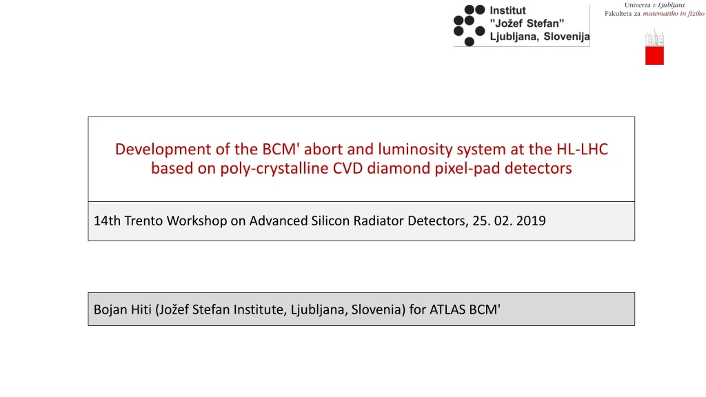
Development of the BCM' abort and luminosity system at the HL-LHC based on poly-crystalline CVD diamond pixel-pad detectors 14th Trento Workshop on Advanced Silicon Radiator Detectors, 25. 02. 2019 Bojan Hiti (Jožef Stefan Institute, Ljubljana, Slovenia) for ATLAS BCM'
ATLAS BCM and BCM' • Current ATLAS abort system: Beam Condition Monitor (BCM) • 2 stations 6.25 ns from IP • Dumps the LHC beam if ATLAS endangered (scattered beam – out of time measurements ± 12.5 ns) • Also used for luminosity measurement • 10 x 10 mm2 single pad pCVD diamond sensor occupancy at high pile-up is problematic (1.5 MIPs / ppcollision) • After HL-LHC upgrade (2024—2026) luminosity will increase by factor 5 z = ±184 cm, r = 55 mm, η= 4.2 collisions in-time can damage the detector background out of time by 12.5 ns Robust solution for HL-LHC BCM' (BCM Prime) BCM'
BCM' upgrade for HL-LHC • pCVD diamond sensor, segmented into 8 pads flexible acceptance • Custom analogue front end BCM' ASIC(designed by OSU) • 65 nm TSMC process, 4 readout channels • Separate front end functionality for Abort (high signals) and Luminosity (low noise) • Current amplifier; < 1 ns rise time, fast (∼10 ns) baseline restoration • Desired sub-ns time resolution for beam diagnostics • Large pitch bump bonding or wire bonding • First prototypes available in September 2018 • Presenting first results from beam tests at CERN SPS and PSI in October 2018 5 mm 5 mm ASIC ASIC diamond thickness 500 μm BCM'
CERN H6 test beam • CERN SPS H6 test beam: 120 GeV hadrons • KarTel (Mimosa) beam telescope • Tracking resolution ≈ 3 μm • DRS 4 analog readout • 3 GS/s acquisition rate, 700 MHz bandwidth • DUT: • + 1000 V bias voltage • DUTs pumped with Sr90 before measurements • Output oscillated if more than one channel per chip active Recorded two channels per run • Dataset: • All channels measured (separate runs) • several 10k tracks per channel DUT 3 planes + timing + ROI 3 planes BCM'
Signals and pick-up baseline of ch. 1 & 2 offset by 0.05 V for clarity • Large pick-up from the setup/environment • Same shape in all channels Mitigation by subtracting two waveforms • (ch1 – ch2) or (ch2 – ch1) depending on track position • Pick-up reduced by factor 2 ch. 1 ch. 2 ch. 1 – ch. 2 Noise before subtraction Noise after subtraction BCM'
Signal measurement • Average waveform of 1000 acquisitons • Select an integration window around the peak [tmin, tmax] • Signal = Integral around the peak • Long integration window [– 6 ns, 6 ns] to mitigate for noise • Hit criterium: signal threshold = 4σ above noise Noise spectrum +4σ noise level varies by factor 2, depending on the channel BCM'
Efficiency measurement Chip 2 channel 1 (1000 V) + 1000 V Efficiency Chip 2 ch. 1 Signal Spectrum • > 99 % hits above threshold • Measured in the fiducial region at + 1000 V • MPV = 7.5 mV, mean 9.8 mV • Noise RMS = 0.5 mV • S/N ratio (mean) ≈ 20 avg. eff. 99.0 % at thr 4σ Noise Spectrum Tracks through sample ≈ 25 tracks per bin BCM'
Chip 2 channel 3 + 1000 V Efficiency Chip 2 ch. 3 Signal Size Chip 2 ch. 3 U (V) Signal Spectrum • High resolution run on a small pad • Efficiency > 99 % in fiducial region at thr. 4σ • Signal size varies with position (pCVD diamond) • Should average out over large pad thr 2.3 mV BCM'
PSI test beam • High Intensity Proton Accelerator (HIPA) at PSI, beam line PiM1, 260 MeV/cpions • PSI beam telescope (150 x 100 μm pixels) + multiple scattering lower resolution • DRS 4 readout, modifications to reduce ringing • Measurements at positive and negative bias voltage: ± 200 V, ± 300V (sample 1), ± 500 V, ± 1000V (sample 2) Thanks to ETH for measurements and analysis! BCM'
Waveforms at PSI • Much lower noise than at CERN – no pickup • ∼1.4 ns Average rise time (20 % – 80 %), • DRS 4 analog bandwidth (700 MHz) may be the limiting factor in the rise time measurement • Baseline restoration after 10 ns • Analysis: Integration time [—1.5 ns, 3 ns] VBias = +200 V VBias = –200 V BCM'
Signal Rise Time • Rise time (20 % – 80 %) ≈ 1 ns • Improves with bias voltage – very few outliers at 1000 V + 1000 V + 300 V BCM'
Charge measurement + 200 V • Charge measurement in fiducial region • 10 % difference for different sign of Vbias at low voltages (0.4 V/μm) • Distribution fitted with convoluted Landau + gaussian • Noise distribution independent of bias voltage, offset is a feature of DRS 4 + 200 V - 200 V BCM'
Signal spectra at 1000 V • At 1000 V signal spectrum is the same for both polarities • Small pedestal – due to low tracking resolution + 1000 V MPV 37.2 Mean 45 – 1000 V MPV 36.7 Mean 45 σ = 1.3 BCM'
Signal summary Diamond 1 Diamond 2 Mean Mean (Mean) S/N ratio = mean signal / noise RMS At highest bias voltages S/N ≈ 40 (mean) Timing resolution: trise / (S/N) = 1.4 ns / 40 = 35 ps very promising BCM'
Efficiency vs. threshold • Efficiency improves from 300 V (0.7 V/μm) 1000 V (2 V/μm) • Inefficiency in part due to low tracking resolution + 300 V + 1000 V typical threshold BCM'
Interchannel coupling • Couplings to the neighbour pad observed – cross talk on the sensor suspected • Similar behaviour observed at SPS • Small signals every time a particle hits the neighbour pad + 1000 V Neighbour pad BCM'
Toward the BCM' module • Module = Sensor + analogue front end + digitization + data transmission • Use "existing" components: • PicoTDC: time-to-digital converter (TDC) developed by CERN • Compatible with lpGBT • 65 nm TSMC process • 12 ps inherent time resolution • 32 channels, selectable between measurement of • Time of arrival • Time over threshold • BCM' requires 16 channels + PicoTDC + lpGBT BCM'
Summary and outlook • Successfully demonstrated functionality of the first BCM' front end prototype • > 99 % efficiency measured in the test beam • S/N (mean) = 40 before irradiation • Good timing performance • Rise time 1.4 ns • Baseline restoration 10 ns • < 100 ps timing resolution is already achievable • Further analogue front end submissions planned • Module production using common components: PicoTDC, lpGBT BCM'
BACKUP BCM'
Chip 1 ch. 2 + Chip 2 ch. 2 + 1000 V Signal Size Chip 2 ch. 2 Efficiency Chip 2 ch. 2 Efficiency Chip 1 ch. 1 Cross talk ? • Observed cross talk on the sample • Separate readout chips, so cross-talk most likely from the sensor • Noise level larger with larger pads 2x higher threshold, efficiency slightly lower BCM'