Download
1 / 47
540 likes | 968 Views
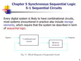
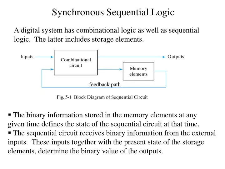
Synchronous Sequential Logic. A digital system has combinational logic as well as sequential logic. The latter includes storage elements. feedback path. The binary information stored in the memory elements at any given time defines the state of the sequential circuit at that time.

E N D
Synchronous Sequential Logic A digital system has combinational logic as well as sequential logic. The latter includes storage elements. feedback path • The binary information stored in the memory elements at any given time defines the state of the sequential circuit at that time. • The sequential circuit receives binary information from the external inputs. These inputs together with the present state of the storage elements, determine the binary value of the outputs.
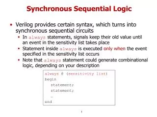
Synchronous Sequential Logic • A synchronous sequential circuit employs signal that affect the • storage elements only at discrete instants of time. • Synchronization is achieved by a time device called clock • generator that provides a periodic train of clock pulses. • Storage elements that are used in clocked sequential circuits • are called flip-flops. • A flip flop is a a binary storage device capable of storing one • bit of information.
Synchronous Clocked Sequential Logic The outputs can come either from the combinational circuit or from the flip-flops or both. The flip-flops receive their inputs from the combinational circuit and a clock signal. The state of the flip-flops can change only during a clock pulse transition.
LATCHES The most basic types of flip-flops are the latches that operate with signal levels. Latches are the building blocks of all flip-flops. undefined state Under normal conditions, both inputs of the latch remain 0 unless the state has to be changed. When S = 1 latch to ‘set’ state: Q = 1, Q’ = 0. Before R is reset to 1, S must go back to 0 to avoid the occurrence of an undefined state with both outputs = 0
SR LATCH with NAND undefined state • SR latch with NAND gates requires a 0 signal to change its state. • The inputs signals for the NAND-latch are the complement values • used for the NOR latch.
SR LATCH with Control Input • The control input C determines when the state of the latch can • be changed. • When C = 0, the output of the NAND gates stays at 1 No change • in state. • When S = 1, R = 0, C = 1 ‘set’ state • When S = 0, R = 0, C = 1 no change in state • When S = 0, R = 1, C = 1 ‘reset’ state
D LATCH D latch eliminates the undesirable condition of the indeterminate state that occurs in the SR latch (Q = Q’ = 1). If D = 1, Q= 1 ‘set’ state If D = 0, Q= 0 ‘reset’ state
Flip-Flops • A flip-flop is a state of a latch that can be switched by momentary • change in the control input. • This momentary change is called a trigger and the transition it causes • is said to trigger the flip-flop. • The D-latch is a flip-flop that is triggered every time the pulse goes • to a high or logic level 1. • As long as the input pulse remains at this level, any changes in the • input data will cause a change in the output and the state of the latch.
Edge-Triggered D Flip-Flop First latch is called Master and second the Slave The circuit samples the D input and changes its output at the negative edge of the clock, CLK. When the clock is 0, the output of the inverter is 1. The slave latch is enabled and its output Q is equal to the master output Y. The master latch is disabled (CLK = 0). When the CLK changes to 1, D input is transferred to the master latch. The slave remains disabled as long as C is 0. Any change in the input changes Y, but not Q. The output of the flip-flop can change when CLK makes a transition 1 0
Positive-Edge-Triggered Flip-Flop • Edge triggered D flip flop uses three SP latches • Two latches respond to external D (Data) and CLK (Clock) inputs • Third latch provides the output for the flipflop • If D = 0 when CLKR 0, Q = 0: ‘reset state’ • If D changes while CLK is high flip-flop will not respond to the change. • When CLK , R1, flip-flop will be in the same state (no change in output). • If D = 1 when CLK , S 0, Q = 1: ‘set state’
Edge-Triggered Flip-Flop: Graphic Symbols The most economical and efficient flip-flop constructed is the edge-triggered D flip-flop since it requires the smallest number of gates. Other types of flip-flops as JK Flip Flop and T flip fop can be constructed by using D flip flop and external logic
D-Flip Flop with Asynchronous Reset • Used to force flip flop to a particular state independent of the clock • Input that sets flip flop to 1 is called Preset or Direct Set • Input that sets flip flop to 0 is called Clear or Direct Reset
JK Flip-Flop • JK flip-flop is capable of performing: set to 1, reset to 0, or • complementing its output: • The J input sets the flip-flop to 1. • The K input resets the flip-flop to 0. • When J and K are enabled, the output is complemented.
JK Flip-Flop When J = 1 and K = 0, D = 1 next clock edge sets output to 1. When J = 0 and K = 1, D = 0 next clock edge resets output to 0. When J = 1 and K = 1, D = Q’ next clock edge complements output. When J = 0 and K = 0, D = Q next clock edge leaves output unchanged.
T Flip-Flop A T (toggle) flip-flop is a complementing flip-flop and can be obtained from a JK flip-flop when the two inputs are tied together.When T=0 (J=K=0) a clock edge does not change the output When T=1 (J=K=1) a clock edge complements the output When T = 0 D = Q and no change in output When T = 1 D = Q’ and the output complements
Characteristic Tables and Equations Q(t) = present state Q(t+1) = next state after one clock period J KQ(t+1) 0 0 Q(t) No change 0 1 0 Reset 1 0 1 Set 1 1 Q’(t) Complement TQ(t+1) 0 Q(t) No change 1 Q’(t) Complement DQ(t+1) 0 0 Reset 1 1 Set
Analysis of Clocked Sequential Circuits The behavior of a clocked sequential circuit is determined from the inputs, outputs, and the state of its flip-flops. • State Equation • A state equation (transition equation) specifies the next state as a • function of the present state and inputs. • State Table • A state table (transition table) consists of: present state, input • next state and output. • State Diagram • The information in a state table can be represented graphically in • a state diagram. The state is represented by a circle and the transitions • between states are indicated by directed lines connecting the circles.
Analysis of Clocked Sequential Circuits Analysis Procedure • Determine the flip-Flop input equations in terms of the present • state and input variables. • Substitute the input equations into the flip-flop characteristic • equation to obtain the state equations. • 3. Use the corresponding state equations to determine the next state • values in the state table.
Example of a Sequential Circuit State Equations (t+1) next state of the flip-flop one clock edge later. Since all variables are function of preset state, we can omit designation (t) after every variable Flip-flop input equations (excitation equations)
Example of a Sequential Circuit (continued) Present Next StateInputStateOutput A B x A B y 0 0 0 0 0 0 0 0 1 0 1 0 0 1 0 0 0 1 0 1 1 1 1 0 1 0 0 0 0 1 1 0 1 1 0 0 1 1 0 0 0 1 1 1 1 1 0 1
Example of a Sequential Circuit (continued) PresentNext StateInputStateOutput A B x A B y 0 0 0 0 0 0 0 0 1 0 1 0 a 0 1 0 0 0 1 0 1 1 1 1 0 b 1 0 0 0 0 1 1 0 1 1 0 0 c 1 1 0 0 0 1 1 1 1 1 0 1 c a b a: When the sequential circuit is in present state 00 and the input is 1, the output is 0. After the next clock cycle, the circuit goes to the next state 01. b: When the sequential circuit is in present state 01 and the input is 1, the output is 0. After the next clock cycle, the circuit goes to the next state 11. c: No change in state.
Example of Sequential Circuit with JK Flip-Flops 1. Flip-Flop input equations: Just by looking at the circuit
Example of Sequential Circuit with JK FF (continued) J KQ(t+1) 0 0 Q(t) No change 0 1 0 Reset 1 0 1 Set 1 1 Q’(t) Complement STEP1 Flip-Flop input equations: Q(t) Q(t+1) Present Next Flip-Flop State Input State Inputs A B x A B 0 0 0 0 1 0 0 1 0 0 0 1 0 0 0 0 0 1 0 1 0 1 1 1 1 1 0 0 1 1 1 0 1 0 0 1 1 0 0 1 1 0 0 1 1 1 0 1 1 0 0 0 0 0 1 1 0 0 0 1 1 1 1 1 1 1 1 1 1 0 0 0 Step 5 STEP2- Based on FF Input Equation STEP3 Based on Characteristic table STEP4 Based on K-Map
Example of Sequential Circuit with T Flip-Flops 1. Flip-Flop input equations: Just by looking at the circuit STEP6 Based on State Diagram
Example: T Flip-Flops circuit (continued) • Present INPUTS Next OUTPUTS • State STATE • A B X A B Y • 0 0 0 0 0 0 • 0 0 1 0 1 0 • 0 1 0 0 1 0 • 0 1 1 1 0 0 • 1 0 0 1 0 0 • 1 0 1 1 1 0 • 1 0 1 1 1 • 1 1 1 0 0 1 TQ(t+1) 0 Q(t) No change 1 Q’(t) Complement STEP4 Based on Step1 STEP1 STEP3 Based on Characteristic table Sequential Circuit state equations STEP5 Based on K-Map
State Reduction Goal: reduce the number of states while keeping the external input-output requirements unchanged. State reduction example: a: input 0 output 0, circuit stays in same state a a:input 1 output 0, circuit goes to state b b: input 0 output 0, circuit goes to state c c: input 1 output 0, circuit goes to state d
State Reduction Present StateNext StateOutput x = 0 x = 1 x = 0 x = 1 a a b 0 0 b c d 0 0 c a d 0 0 d e f 0 1 e a f 0 1 f g f 0 1 g a f 0 1
State Reduction State Reduction Algorithm: Two states are equivalent if, for each member of the set inputs, they give the same output and send the circuit to the same state or equivalent state. Present StateNext StateOutput x = 0 x = 1 x = 0 x = 1 a a b 0 0 b c d 0 0 c a d 0 0 d e f 0 1 e a f 0 1 f g f 0 1 g a f 0 1 e equivalent states row with present state g is removed, and state g is replaced by state e each time it occurs.
State Reduction State Reduction Algorithm: Two states are equivalent if, for each member of the set inputs, they give the same output and send the circuit to the same state or equivalent state. Present StateNext StateOutput x = 0 x = 1 x = 0 x = 1 a a b 0 0 b c d 0 0 c a d 0 0 d e f 0 1 e a f 0 1 f e f 0 1 d d equivalent states row with present state f is removed, and state f is replaced by state d each time it occurs.
State Reduction Present StateNext StateOutput x = 0 x = 1 x = 0 x = 1 a a b 0 0 b c d 0 0 c a d 0 0 d e d 0 1 e a d 0 1
State Coded Binary Assignment • While designing a circuit, it is necessary to assign coded binary values to states. Can assign Binary, Gray Code etc… • For a circuit with m States, the Code must contain n bits where 2n >=m. For example with three bits we can assign codes to eight bits • If number of states is less, the remaining state is unused • Unused states are treated as Don’t Care conditions • Since Don’t care can result in simple circuits, it is more likely that circuit will require fewer combinational gates Present StateNext StateOutput x = 0 x = 1 x = 0 x = 1 a 000 a 000 b 001 0 0 b 001 c 010 d 0110 0 c 010 a 000 d 011 0 0 d 011 e 100 d 011 0 1 e 100 a 000 d 011 0 1 Reduced State Table with Binary Assignment
Sequential Circuits: Design Procedure • Recommended Design Steps • Derive the state diagram from the word description and the • specifications of the desired operation. • Reduce the number of states if necessary. • Assign binary values to the states. • Obtain the binary coded-state table. • Chose the type of flip-flops to be used. • Derive the simplified flip-flop input and output equations. • Draw the logic diagram.
Sequence Detector Sequential Circuit Design a circuit that detects three or more consecutive 1’s in a string of bits using D Flip-Flops. • Start with state S0 • If the input is 0 circuit stays in the same state • If the next input is 1 circuit goes to S1 to indicate that 1 was detected • If the next input is 1 circuit goes to S2 to indicate that the arrival of two • consecutive 1’s. • But if the input were 0 circuit goes back to S0. • The third consecutive 1 sends the circuit to S3. • If more 1 are detected circuit stays in S3. Draw the state diagram. STEP1
Sequence Detector Sequential Circuit • State table is derived directly from the state diagram. • We choose 2 D Flip-Flops (outputs A, B) • There is one input x and one output y Present State Next State Input Output D flip-flop state Equations: STEP1 Based on State Diagram STEP3
Sequence Detector Sequential Circuit • Obtain the simplified functions from the K-Maps: STEP3-continued
Design using JK Flip-Flops Flip-Flop Excitation table: Design procedure for sequential circuit with JK Flip Flop is same a D Flip Flop, except the input equation must be evaluated from the present-state to next-state transition derived from excitation table
Design using JK Flip-Flops In order to determine the input equations for the JK flip-flops, it is necessary to derive a functional relationship between the state table and the input equations. Present State Next State Flip-Flop inputs Input STEP 1 Truth Table derived specification STEP 2 Derived from Excitation Table Flip-Flop Excitation table:
Design using JK Flip-Flops STEP 3
Design using JK Flip-Flops STEP 4
Design using T Flip-Flops Flip-Flop Excitation table: Design procedure for sequential circuit with T Flip Flop is same a D Flip Flop, except the input equation must be evaluated from the present-state to next-state transition derived from excitation table
Design using T Flip-Flops COUNTER= A sequential cct that goes through a prescribed sequence of states upon the application of i/p pulses is called a counter.