Download
1 / 33
330 likes | 523 Views
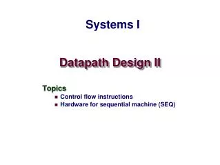
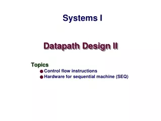
99-1 Under-Graduate Project Design of Datapath Controllers. Speaker: Shao-Wei Feng Adviser: Prof. An-Yeu Wu Date: 2010/10/14. Outline. Sequential Circuit Model Finite State Machines Useful Modeling Techniques. Inputs. Outputs. Combinational Logic. Memory Elements. Current State.

E N D
99-1 Under-Graduate ProjectDesign of Datapath Controllers Speaker: Shao-Wei Feng Adviser: Prof. An-Yeu Wu Date: 2010/10/14
Outline • Sequential Circuit Model • Finite State Machines • Useful Modeling Techniques
Inputs Outputs Combinational Logic Memory Elements Current State Next State clock Model of Sequential Circuits • System outputs depend not only on current input • Depend on inputs • Depend on current state • Fundamental components • Combinational circuits • Memory elements
Types of Memory Elements • Flip-Flop • Latch • Registers • Others • Register Files • Cache • Flash memory • ROM • RAM
D-FF vs. D-Latch • FF is edge sensitive(can be either positive or negative edge) • At trigger edge of clock, input transferred to output • Latch is level sensitive(can be either active-high or active-low) • When clock is active, input passes to output (transparent) • When clock is not active, output stays unchanged Latch in out in out D Q E D Q FF clk clk in in clk clk out out
Combinational Logic Td FF FF clk Tcycle Tcq Td Tsetup FF Based, Edge Trigger Clocking • Td = delay of combinational logic • Tcycle = cycle time of clock • Duty cycle does not matter • Timing requirements for Td • Tdmax < Tcycle –Tsetup – Tcq no setup time violation • Tdmin > Thold – Tcq no hold time violation
Latch Based, Single Phase Clocking • Pulse Mode clocking • Tcycle = cycle time of clock; Tw = pulse width of clock • Timing requirements for Td • Tdmax < Tcycle –Tdq data latched correctly • Tdmin > Tw – Tdq no racing through next stage Combinational Logic Td Latch Latch clk Tcycle Tw Tdq Td
Comparison • Flip-Flop Based • Larger in area • Larger clocking overhead (Tsetup, Tcq) • Design more robust Only have to worry about Tdmax Tdmin usually small, can be easily fixed by buffer • Pulse width does not matter • Latch Based Single Phase • Smaller area • Smaller clocking overhead ( only Tdq) • Worry about both Tdmax and Tdmin • Pulse width does matter (unfortunately, pulse width can vary on chip)
D Flip-Flop with Positive-Edge Clock D Q module flop (Q, D, C, S, R); output Q; // Flip-Flop Output input D; // Data Input input C; // Positive Edge Clock input E; // Clock Enable reg Q; // Register Type always @(posedge C) begin if (E)// Check Enable Q <= D; end endmodule C D Q E C
S R D Flip-Flop with Positive-Edge Clock module flop (Q, D, C, S, R); output Q; // Flip-Flop Output input D; // Data Input input C; // Positive Edge Clock input R; // Asynchronous Reset input S; // synchronous Set reg Q; // Register Type always @(posedge C or negedge R) begin if (!R) Q <= 1’b0; else if (S) Q <= 1’b1; else Q <= D; end endmodule D Q C
Latch Issue • Latches are to be avoidedin most designs! • Prone to timing violations and glitches • Cannot implement synchronous operations • Common mistakes that generate latches always@( a or b ) begin if( a == 2’d0 ) z = 1’b0; else if( a == 2’d1 ) z = ~b; else if( a == 2’d2 ) z = b; // no else statement!end always@( a or b ) begin case( a ) 2’d0: z = b; 2’d1: z = ~b; 2’d2: z = c; // no default statement! endcaseend always@( /*forget edge!*/ clk ) begin z <= b;end
What is FSM • A model of computation consisting of • a set of states, (limited number) • a start state, • input symbols, • a transition function that maps input symbols and current states to a next state.
Elements of FSM • Memory Elements (ME) • Memorize Current States (CS) • Usually consist of FF or latch • N-bit FF have 2n possible states • Next-state Logic (NL) • Combinational Logic • Produce next state • Based on current state (CS) and input (X) • Output Logic (OL) • Combinational Logic • Produce outputs (Z) • Based on current state • Based on current state and input
Mealy Machine • Output (Z) is function of both • Input (X) • Current state (CS)
Moore Machine • Output(Z) is function of • Current state (CS) only
Mealy Finite State Machine A serially-transmitted BCD (8421 code) word is to be converted into an Excess-3 code. An Excess-3 code word is obtained by adding 3 to the decimal value and taking the binary equivalent. Excess-3 code is self-complementing [Wakerly, p. 80], i.e. the 9's complement of a code word is obtained by complementing the bits of the word.
State Transition Graph Mealy Finite State Machine The serial code converter is described by the state transition graph of a Mealy FSM. • The vertices of the state transition graph of a Mealy machine are labeled with the states. • The branches are labeled with (1) the input that causes a transition to the indicated next state, and (2) with the output that is asserted in the present state for that input. • The state transition is synchronized to a clock. • The state table summarizes the machine's behavior in tabular format.
Design of a Mealy Finite State Machine To design a D-type flip-flop realization of a FSM having the behavior described by a state transition graph, (1) select a state code, (2) encode the state table, (3) develop Boolean equations describing the input of a D-type flip-flop, and (4) using K-maps, optimize the Boolean equations.
Design of a Mealy Finite State Machine Note: We will optimize the equations individually. In general - this does not necessarily produce the optimal (area, speed) realization of the logic. We'll address this when we consider synthesis.
Design of a Mealy Finite State Machine Realization of the sequential BCD-to-Excess-3 code converter (Mealy machine):
Design of a Mealy Finite State Machine Simulation results for Mealy machine:
Modeling FSM in Verilog • Sequential Circuits • Memory elements of States (CS) • Combinational Circuits • Next-state Logic (NL) • Output Logic (OL) • Three coding styles • (1) Separate CS, OL and NL • (2) Combines NL+ OL, separate CS • (3) Combine CS + NL, separate OL
Coding Style 1 – Separate CS, NL, OL • CS • NL • OL
Coding Style 2 – Combine NL+OL; Separate CS • CS • NL+OL
Coding Style 3 – Combine CS+NL; Separate OL • CS+NL • OL
FSM Architecture Modeling Build combinational and sequential parts separately! Coding style 2 fits this architecturevery well!
Conclusion • FSM Design • Partition FSM and non-FSM logic • Partition combinational part and sequential part • Use parameter to define names of the state vector • Assign a default (reset) state