Download
1 / 38
1.75k likes | 4.3k Views
CMOS Fabrication. EMT 251. Objectives. To discussed the fundamentals of CMOS fabrication steps. To examined the major steps of the process flow. To overview the cross section view of a circuit. Chip making Process. CMOS. PMOS. NMOS. Introduction. MOSFET. MOSFET. Gate. Drain. Source.

E N D
CMOS Fabrication EMT 251
Objectives • To discussed the fundamentals of CMOS fabrication steps. • To examined the major steps of the process flow. • To overview the cross section view of a circuit
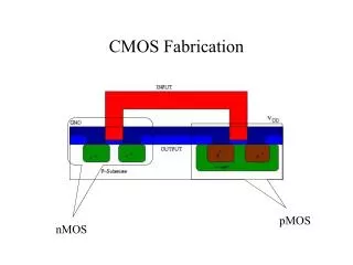
CMOS PMOS NMOS Introduction MOSFET
MOSFET Gate Drain Source • Metal Oxide Semiconductor Field Effect Transistor • Source (Arsenic, Phosphorous, Boron) • Drain (Arsenic, Phosphorous, Boron) • Gate (Aluminum, Polysilicon)
P-type substrate NMOS • N-type dopant for Source & Drain • Inversion layer is formed to conduct electricity
P-type substrate NMOS • N-type dopant for Source & Drain • Inversion layer is formed to conduct electricity
N-type substrate PMOS • P-type dopant for Source & Drain • Inversion layer is formed to conduct electricity
N-type substrate PMOS • P-type dopant for Source & Drain • Inversion layer is formed to conduct electricity
A combination of both NMOS & PMOS technology CMOS • Most basic example: inverter
WELL FORMATION ISOLATION FORMATION TRANSISTOR MAKING INTERCONNECTION PASSIVATION PROCESS FLOW
CMOS FABRICATION PROCESSwell formation • Start with clean p-type substrate (p-type wafer)
CMOS FABRICATION PROCESSwell formation • Grow epitaxy layer (made from SiO2) as mask layer for well formation
CMOS FABRICATION PROCESSwell formation • By *photolithography and etching process, well opening are made *photolithography and etch processes are shown in next slides Well will be formed here
Photolithography (CED) photoresist Si02 • Photoresist coating (C) • Masking and exposure under UV light(E) • Resist dissolved after developed (D) • Pre-shape the well pattern at resist layer P-substrate UV light mask Opaque area P-substrate Transparent area
etching • Removing the unwanted pattern by wet etching • Resist clean • Desired pattern formed P-substrate P-substrate
CMOS FABRICATION PROCESSwell formation • Ion bombardment by ion implantation • SiO2 as mask, uncovered area will exposed to dophant ion Phosphorus ion
CMOS FABRICATION PROCESSisolation formation • Increase SiO2 thickness by oxidation at high temperature • Oxide will electrically isolates nmos and pmos devices Thick oxide
CMOS FABRICATION PROCESStransistor making • By photolithography and etching process, pmos and nmos areas are defined pmos will be formed here nmos will be formed here LOCOS (isolation structure)
CMOS FABRICATION PROCESStransistor making • Grow very thin gate oxide at elevated temperature in very short time Gate oxide
CMOS FABRICATION PROCESStransistor making • Deposit polisilicon layer polisilicon
CMOS FABRICATION PROCESStransistor making • Photolithography (photo) and etching to form gate pattern gate
CMOS FABRICATION PROCESStransistor making Arsenic ion • Photo process to define the nmos’s active (source and drain) area and VDD contact • Ion implantation with Arsenic ion for n+ dophant. • Photoresist and polisilicon gate act as mask photoresist
CMOS FABRICATION PROCESStransistor making • Nmos’s Source and drain with VDD contact formation • Resist removal VDD contact source drain
CMOS FABRICATION PROCESStransistor making • Photo process to define the GND contact and pmos’s active area (source and drain) • Ion implantation with boron ionto have p+ dophant • Photoresist and gate act as mask Boron ion photoresist
CMOS FABRICATION PROCESStransistor making • Pmos’s source and drain formation with GND contact • Resist removal GND contact Pmos’s drain Pmos’ source
CMOS FABRICATION PROCESSinterconnection • Deposit SiO2 layer through out wafer surface SiO2
CMOS FABRICATION PROCESSinterconnection • Photo and etching process to make contact contact
CMOS FABRICATION PROCESSinterconnection • Metal 1 deposition throughout wafer surface Metal 1
CMOS FABRICATION PROCESSinterconnection • Photo and etching processes to pattern interconnection
A’ A N-well Metal 1 oxide p+ n+ n+ p+ p-substrate n+
B B’ Assignment
GLOSSARY • Photolithography (photo) • Process of transferring pattern on mask to photoresist layer on wafer surface (pre-pattern the chip) • Etching • Process of permanently removed the unwanted part of design on wafer surface to get the desired pattern • Diffusion • Process of introducing dophant layer by movement of dophant atoms from high concentration to low concentration area at high temperature • Ion implantation • Process of introducing dophant layer by bombardment of high energy dophant ion in high electric field chamber • Oxidation • Process of growing thick or thin SiO2 layer depend on oxide application • CMP • Process to physically grind flat to have a planar surface for better exposure at photo process.