Download
1 / 27
270 likes | 457 Views
Description of pixel designs in Mimosa22. Andrei Dorokhov Institut Pluridisciplinaire Hubert Curien (IPHC) Strasbourg, France. 03/04/2008. e-mail address: Andrei.Dorokhov@IReS.in2p3.fr. Pixel designs. Standard and Radiation tolerant nwell diode designs Different schematic concepts:

E N D
Description of pixel designs in Mimosa22 Andrei Dorokhov Institut Pluridisciplinaire Hubert Curien (IPHC) Strasbourg, France 03/04/2008 e-mail address: Andrei.Dorokhov@IReS.in2p3.fr
Pixel designs • Standard and Radiation tolerant nwell diode designs • Different schematic concepts: • Reset diode and standard amplifier (like in Mimosa8) • Reset diode and amplifier with improved load • Continuously biased (self-biased) from feedback and amplifier with improved load (like in Mimisa15 test structures and Mimosa16) • Reset diode from feedback, time variant feedback, amplifier with improved load (similar to Mimosa1819 test structures) • Reset diode from feedback, time variant feedback, standard amplifier • CDS with clamping capacitance
Nwell diode designs • Size from 3.4 um x 3.4 um - to 4.5 um x 4.5 um • Standard with thick oxide around Nwell • Radiation tolerant with thin gate oxide around Nwell
Amplifier schematics (1): standard common source + reset bias reset M3 out M1 Id in M2 signal current Nwell / Pepi
Amplifier schematics (2): improved common source + reset M4 bias reset M3 out M1 Id in M2 Nwell / Pepi signal current
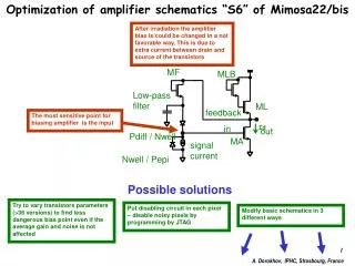
Amplifier schematics (3): improved common source + continuously biased from feedback (self-biased) M4 M5 Low-pass filter out M3 feedback out Id Pdiff / Nwell in M2 Nwell / Pepi signal current
Amplifier schematics (4): improved common source + reset from feedback (time-variant feedback) reset M4 M5 M3 out Time-variant feedback Id in M2 Nwell / Pepi signal current
Amplifier schematics (5): standard common source + reset from feedback (time-variant feedback) reset M4 M3 out Time-variant feedback Id in M2 Nwell / Pepi signal current
(1,2) reset (and amplifier bias) from constant voltage • - may be difficult to find working point due to CMOS process variation • - diode leakage current dispersion after irradiation may significantly degrade performance • (3) self-biased from feedback • + performances should be more stable to process variation • + diode leakage is compensated by forwardly biased diode • - “pedestal memory effect” from previous hit, even removed after CDS, changing the performance of amplifier • (4,5) reset from feedback • + more stable performances for process variation • - diode leakage current dispersion after irradiation will significantly degrade performance Summary of pixel concepts
Simulation results Simulation with Spectre, parasitic capacitances for diodes, metal lines and transistors are extracted by Frédéric Morel
Short results summary of measurements and analysis from Mathieu Goffe: • S6, S7, S8, S9, S10, S12, S13, S15, S16, S17 are working fine at standard conditions at 100MHz clock • For working pixels the charge collection in seed ~30%, cluster 3x3: 60-80%, in cluster 5x5 : 80-90%, noise from 10e to 13e • The other pixels have to be investigated further – one need to vary the frequency, readout pattern, analogue voltages – at least to understand the reason why they don’t show good performances seen in simulations (this is foreseen for the end of April) • However, there are at least few working amplifier concepts:1,2,3. • Two designs S6 and S10 have different concepts: reset and self-biased from feedback, they are featured with radiation tolerant version of nwell diode -> one can have close look at their performances Measurement results
Measurement results for S6 and S10 S6, pedestal dispersion + noise S10, pedestal dispersion + noise
Measurement results for S6 and S10 S6, pedestal mean dispersion S10, pedestal mean dispersion
Measurement results for S6 and S10 S6, pedestal sigma dispersion S10, pedestal sigma dispersion
Influence of pixel hit frequency • Designs with reset are not sensitive to “memory” effect – charge is always restored to a fixed value • Continuously biased diode will store some fraction of charge from previously incident particle, even if the signal completely reconstructed after CDS, there is “internal memory” in the nwell diode -> charge is accumulated and circuit can go to non-linear state
Influence of pixel hit frequency: simulation • Single pixel hit frequency 2Hz for 30um x 30um pitch • Noise – Gaus : SIGMA=15 e • Signal - Landau distribution: MPV=200e, SIGMA=50e • Initial nwell diode voltage 0.7 V • Amplifier gain -10, offset 1.1 V • Frame readout (integration time) time 160 us (==1000 pixels in column, 100MHz clock)
Conclusions • There two pixel candidates for PHASE1: designs S6 and S10 • Radiation hardness and hit frequency issues has to be carefully studied for these candidates – one of those may be not suitable for real experiment…