Download
1 / 15
190 likes | 346 Views
VLSI Design CMOS Layout. Engr. Noshina Shamir UET, Taxila. CMOS Layout. Layout design rules describe how small features can be and how closely they can be reliably packed in a particular manufacturing process.

E N D
VLSI Design CMOS Layout Engr. Noshina Shamir UET, Taxila
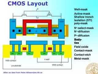
CMOS Layout • Layout design rules describe how small features can be and how closely they can be reliably packed in a particular manufacturing process. • Lambda-based rules are necessarily conservative because they round up dimensions to an integer multiple of lambda. • Designers often describe a process by its feature size. • Feature size refers to minimum transistor length, so lambda is half the feature size. 1: Circuits & Layout
The rules describe the minimum width to avoid breaks in a line, minimum spacing to avoid shorts between lines, and minimum overlap to ensure that two layers completely overlap. • Transistor dimensions are often specified by their Width/Length (W/L) ratio. • In a 0.6 µm process, this corresponds to an actual width of 1.2 µm and a length of 0.6 µm. • In digital systems, transistors are typically chosen to have the minimum possible length because short-channel transistors are faster, smaller, and consume less power. • The power and ground lines are often called supply rails. 1: Circuits & Layout
Layout Design Rules • Metal and diffusion have minimum width and spacing of 4 l . • Contacts are 2 l × 2 l and must be surrounded by 1 l on the layers above and below. • Polysilicon uses a width of 2 l 1: Circuits & Layout
Polysilicon overlaps diffusion by 2 l where a transistor is desired and has a spacing of 1 l away where no transistor is desired. • Polysilicon and contacts have a spacing of 3 l from other polysilicon or contacts. • N-well surrounds pMOS transistors by 6 l and avoids nMOS transistors by 6 l. 1: Circuits & Layout
Simplified Lambda based Design Rules 1: Circuits & Layout
Example: Inverter 1: Circuits & Layout
Example: NAND3 • Horizontal N-diffusion and p-diffusion strips • Vertical polysilicon gates • Metal1 VDD rail at top • Metal1 GND rail at bottom • 32 l by 40 l 1: Circuits & Layout
Stick Diagrams • Stick diagrams help plan layout quickly • Need not be to scale • Draw with color pencils or dry-erase markers 1: Circuits & Layout
Wiring Tracks • A wiring track is the space required for a wire • 4 l width, 4 l spacing from neighbor = 8 l pitch • Transistors also consume one wiring track 1: Circuits & Layout
Well spacing • Wells must surround transistors by 6 l • Implies 12 l between opposite transistor flavors • Leaves room for one wire track 1: Circuits & Layout
Area Estimation • Estimate area by counting wiring tracks • Multiply by 8 to express in l 1: Circuits & Layout
Example: O3AI • Sketch a stick diagram for O3AI and estimate area 1: Circuits & Layout
Example: O3AI • Sketch a stick diagram for O3AI and estimate area 1: Circuits & Layout
Example: O3AI • Sketch a stick diagram for O3AI and estimate area 1: Circuits & Layout