Download
1 / 19
220 likes | 551 Views
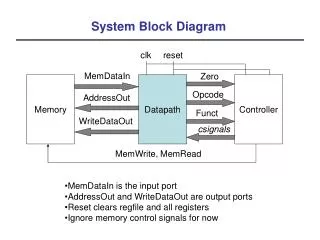
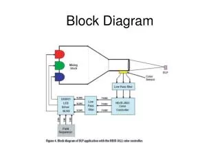
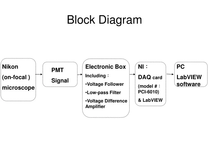
Block Diagram. Nikon (on-focal ) microscope. Electronic Box Including : Voltage Follower Low-pass Filter Voltage Difference Amplifier. NI : DAQ card (model # : PCI-6010) & LabVIEW. PC LabVIEW software. PMT Signal. Operational Amplifier : OP 27. Low noise, low drift, low offset

E N D
Block Diagram Nikon (on-focal ) microscope • Electronic Box • Including: • Voltage Follower • Low-pass Filter • Voltage Difference Amplifier NI: DAQ card (model #:PCI-6010) & LabVIEW PC LabVIEW software PMT Signal
Operational Amplifier:OP 27 • Low noise, low drift, low offset • Supply voltage ( ):±12V (old design) / ±15V (new design)
Voltage Follower Change the output impedance while the output voltage equals to the input one. Vsig Vout
Butterworth Low-pass Filter • Synthesize a fourth-order Butterworth low-pass filter by cascading two second-order low-pass section. • Cut off Frequency: f0 80Hz • Ref:J. Millman, “microelectronics:digital and analog circuits & systems” pp.582-586 (1979) 10 k 1.52 k 10 k 12.35 k 2 k 2 k 2 k 2 k Vout Vsig 1μ 1μ 1μ 1μ
Voltage Difference Amplifier • Amplifying the difference between two inputs by a gain factor. • Here Vref isadjustable offset voltage • Note that this circuit applies to negative signal input (old design) Rf R Vsig Vout +Vcc R Rf Vref -Vcc Vout = (Vref- Vsig)*
Voltage Difference Amplifier • Amplifying the difference between two inputs by a gain factor. • Here Vref isadjustable offset voltage • Note that this circuits applies to positive signal input (new design) Rf +Vcc Vref R Vout -Vcc R Vsig Rf Vout = (Vsig - Vref)*
1.52K (502) Electronic Circuit Layout (old design) 12.35K (503) 10K 10K 1000K 100K 2K 2K 2K 2K +Vcc Signal Output ≦ 5 V 100K 1μ Signal Input (from detector) Signal < 200 mV 1μ 1μ 1000K 1μ (503) -Vcc
1.52K (502) Electronic Circuit Layout (new design) 12.35K (503) 10K 10K 1000K 100K 2K 2K 2K 2K Signal Output ≦ 5 V 100K 1μ Signal Input (from detector) Signal < 200 mV 1μ 1μ 1000K To panel potential meter 1μ
R1 R2 Vsig Vsig Voltage Meter Driver • Non-inverting Amplifier • To drive the voltage meter ( Reason:to match the meter scale ) • Vout = Vin * ( ) = Variable Resistance (50K) Output
Calibrate the Voltage Meter Scale • PMT, Monitor and the Voltage Meter should possess linear relationships • Adjust the gain (ratio of R1 / R2) of the non-inverting amplifier with different PMT values • PMT Voltage Range:0~1000V Monitor Signal Range:0~4V Voltage Meter Reading:0~10V • For example:
Power Line Wiring in the Electronic Box (old design) L:red line N:blue line G:green line G 1 N L 2 switch 3 LNG -V +V com +5V LNG -V +V ±12V +15V
Power Line Wiring in the Electronic Box (new design) L:red line N:blue line G:green line G 1 N L 2 switch 3 LNG -V +V com +5V ±15V
Electronic and Panel Wiring (old design) To Electronic Circuit V+ V- +5V (not used) Vcom +12V -12V +15V Power Supply ±12V Power Supply Connect to the output of the voltage meter driver Connect to the input of the voltage meter driver To Electronic Circuit - + +15V Output (To PMT) Signal Output (To DAQ) PMT Signal Input PMT Voltage Monitor Signal Offset Voltage meter
Electronic and Panel Wiring (new design) To Electronic Circuit +5V (not used) Vcom +15V -15V ±15V Power Supply Connect to the output of the voltage meter driver Connect to the input of the voltage meter driver To Electronic Circuit - + +15V Output (To PMT) Signal Output (To DAQ) PMT Signal Input PMT Voltage Monitor Signal Offset Voltage meter
Electronic Testing • multi-meter: check the circuit before connecting to the power supply. • function generator & oscilloscope: check whether the output of each component satisfies our expectation: a. Each OP Amp should function properly!(make sure the pins have right voltage.) b. Voltage Follower:should be exactly the same with the input. c. Low-pass Filter:should filter out the signals with frequency higher than 80 hz. d. Voltage difference amplifier:should amplify our signals with the designed gain factor.
IN Voltage Meter OUT 1 1 1 OFFSET 1 1 Circuit Layout 1 2 3 4 5 6 7 8 9 10 11 12 13 14 15 16 17 18 19 20 21 22 23 24 25 26 27 28 29 30 • 1 • 2 • 3 • 4 • 5 • 6 • 7 • 8 • 9 • 10 • 11 • 12 • 13 • 14 • 15 • 16 • 17 • 18 • 19 • 20 • 21 • 22 • 23 • 24 • 25 • 26 • 27 • 28 • 29 • 30 :To V+ :To V- :To Vcom (ground) :To the panel :two points connected :wired
Testing the Frequency Response • With fixed amplitude sinusoidal wave signals, we can test how the electronic circuit box low-pass filter responds to the sinusoidal wave frequencies. Function Generator Oscilloscope Freq. OUTPUT Ch.1 Ch.2 Electronic Circuit Box Input Signal Output Signal
Experimental Frequency Response • Input : 100 mV, sinusoidal waves -3 dB 75