Download
1 / 32
330 likes | 554 Views
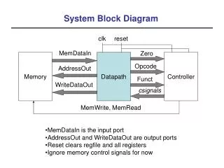
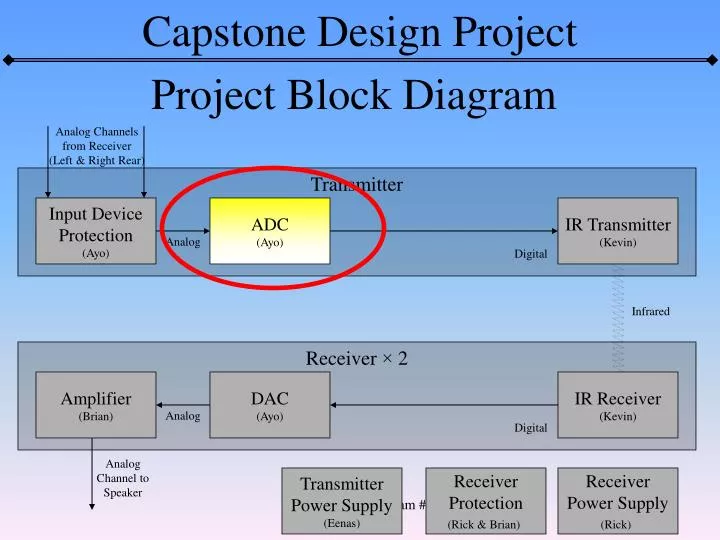
Project Block Diagram. Analog Channels from Receiver (Left & Right Rear). Transmitter. Input Device Protection (Ayo). ADC (Ayo). IR Transmitter (Kevin). Analog. Digital. Infrared. Receiver × 2. Amplifier (Brian). DAC (Ayo). IR Receiver (Kevin). Analog. Digital.

E N D
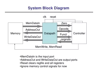
Project Block Diagram Analog Channels from Receiver (Left & Right Rear) Transmitter Input Device Protection (Ayo) ADC (Ayo) IR Transmitter (Kevin) Analog Digital Infrared Receiver × 2 Amplifier (Brian) DAC (Ayo) IR Receiver (Kevin) Analog Digital Analog Channel to Speaker Transmitter Power Supply (Eenas) Receiver Protection (Rick & Brian) Receiver Power Supply (Rick) Ayodeji Opadeyi Team #2
ADC Schematic Ayodeji Opadeyi Team #2
ADC Device Packaging Prototype • Thru Hole Product • Surface mount Ayodeji Opadeyi Team #2
ADC Components Prototype • eight 5% tolerance resistors, ½ W (R1 = 3.9kΩ, R2 = 10kΩ, R5 = 3kΩ) • Two clock circuits • two op-amps • four diodes, ½ W • Four 10µF 20% tolerance capacitors, • Eight 0.1µF 20% tolerance capacitors • 2 Max195 chips (DIP) Product • Eight 5% tolerance resistors, ½ W (R1 = 3.9kΩ, R2 = 10kΩ, R5 = 3kΩ) • Two clock circuits • two op-amps • four diodes, ½ W • Four 10µF 20% tolerance capacitors • Eight 0.1µF 20% tolerance capacitors • 2 Max195 chips (Surface mount) Ayodeji Opadeyi Team #2
ADC Resistor Selection • R1 = 10 kΩ • R2 = 3.9 kΩ • R5 = R1 || R2 = 3k Ω • R7 = 100 Ω • When choosing the above resistors, the noise was considered: vn2 = 4kTRB From the above equation we see that when the resistor is increased, the square of the noise voltage also increases. • The current entering the ADC also has to be minimized, therefore I chose resistors appropriately. With the above considerations in mind, I chose my resistor values in order to have the ADC input current at its minimum, and the noise voltage at its minimum. Ayodeji Opadeyi Team #2
ADC Design Calculation Maximum Voltage Output from Audio Receiver: 8Vrms Maximum Input Analog Voltage to ADC: 4.75Vrms Maximum Gain Signal Conditioner Allowed: 0.594 Ayodeji Opadeyi Team #2
Gain Error due to Resistor Tolerances Ayodeji Opadeyi Team #2
Gain Error (Continued) Ayodeji Opadeyi Team #2
Input Offset Voltage Error Ayodeji Opadeyi Team #2
Input Offset/Bias Current Error Ayodeji Opadeyi Team #2
Gain Error Ayodeji Opadeyi Team #2
Gain Error (Continued) Ayodeji Opadeyi Team #2
ADC Prototype Bill Of Materials Ayodeji Opadeyi Team #2
ADC Product Bill Of Materials Ayodeji Opadeyi Team #2
ADC Analog Block DFM Plan Ayodeji Opadeyi Team #2
ADC Digital Block DFM - DC Drive Analysis Table Ayodeji Opadeyi Team #2
ADC Digital Block DFM - Timing Analysis Table Ayodeji Opadeyi Team #2
System Level Block Diagram Analog Channels from Receiver (Left & Right Rear) Transmitter Input Device Protection ( Ayo) ADC (Ayo) IR Transmitter (Kevin) Analog Digital Infrared Receiver × 2 Amplifier (Brian) DAC (Ayo) IR Receiver (Kevin) Analog Digital Analog Channel to Speaker Transmitter Power Supply (Eenas) Receiver Protection (Rick & Brian) Receiver Power Supply (Rick) Ayodeji Opadeyi Team #2
DAC Schematic Ayodeji Opadeyi Team #2
DAC Device Packaging Prototype • Thru Hole Product • Surface mount Ayodeji Opadeyi Team #2
DAC Components Prototype • eight 5% resistors • Two clock circuits • two op-amps • Four 20% 10µF capacitors • Eight 20% 0.1µF capacitors • 2 Max541 chips (DIP) Product • eight 5% resistors • Two clock circuits • two op-amps • Four 20% 10µF capacitors • Eight 20% 0.1µF capacitors • 2 Max541 chips (Surface mount) Ayodeji Opadeyi Team #2
DAC Resistor Selection • R1 = 10 kΩ • R2 = 3.9 kΩ • R5 = R1 || R2 = 3k Ω • R7 = 10 Ω • R7 was chosen because the data sheet specified it, the other resistors were chosen in order to revert the signal, so I just swapped the ADC resistors. Ayodeji Opadeyi Team #2
Gain Error due to Resistor Tolerances Ayodeji Opadeyi Team #2
Input Offset Voltage Error Ayodeji Opadeyi Team #2
Input Offset/Bias Current Error Ayodeji Opadeyi Team #2
Gain Error Ayodeji Opadeyi Team #2
Gain Error (Continued) Ayodeji Opadeyi Team #2
DAC Prototype Bill Of Materials Ayodeji Opadeyi Team #2
DAC Product Bill Of Materials Ayodeji Opadeyi Team #2
DAC Analog Block DFM Plan Ayodeji Opadeyi Team #2
DAC Digital Block DFM - DC Drive Analysis Table Ayodeji Opadeyi Team #2
DAC Digital Block DFM - Timing Analysis Table • Std = Standard, OC = Open Collector/Drain, TS = Tristate, ST – Schmitt Trigger Ayodeji Opadeyi Team #2