Download
1 / 22
220 likes | 329 Views
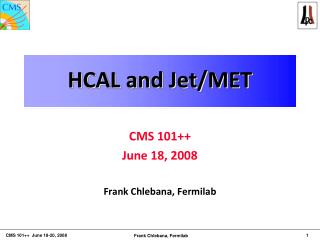
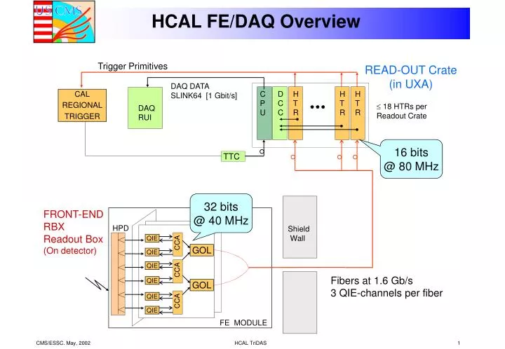
Trigger Primitives. READ-OUT Crate (in UXA). DAQ DATA SLINK64 [1 Gbit/s]. CAL REGIONAL TRIGGER. CPU. D C C. H T R. H T R. H T R. DAQ RUI. 18 HTRs per Readout Crate. 16 bits @ 80 MHz. TTC. 32 bits @ 40 MHz. CCA. CCA. CCA. FRONT-END RBX Readout Box

E N D
Trigger Primitives READ-OUT Crate (in UXA) DAQ DATA SLINK64 [1 Gbit/s] CAL REGIONAL TRIGGER CPU D C C H T R H T R H T R DAQ RUI 18 HTRs per Readout Crate 16 bits @ 80 MHz TTC 32 bits @ 40 MHz CCA CCA CCA FRONT-END RBX Readout Box (On detector) HPD Shield Wall QIE GOL QIE QIE Fibers at 1.6 Gb/s 3 QIE-channels per fiber QIE GOL QIE QIE FE MODULE HCAL FE/DAQ Overview HCAL TriDAS
Readout Crate Components • “BIT3” board • Commercial VME/PCI Interface to CPU • Slow monitoring • HTR (HCAL Trigger and Readout) board • FE-Fiber input • TPs output (SLBs) to CRT • DAQ/TP Data output to DCC • Spy output • TCC/Clock FanOut board • FanOut of TTC stream • FanOut of RX_CK & RX_BC0 for SLBs • DCC (Data Concentrator Card) board • Input from HTRs • Output to DAQ • Spy output Front End Electronics TTC fiber Gbit Ethernet @ 1.6 Gb/s F a n O u t B I T 3 H TR H T R H T R H T R D C C (s) ... D C C 20 m Copper Links 1 Gb/s DAQ Calorimeter Regional Trigger HCAL TriDAS
HCALTRIGGERandREADOUTCard • No functional changes since Dec-2001 • I/O on front panel: • Inputs: Raw data: • 16 digital serial fibers from QIE, 3 HCAL channels per fiber = 48 HCAL channels • Inputs: Timing (clock, orbit marker, etc.) • PECL • Outputs: DAQ data output to DCC • Two connector running LVDS • TPG (Trigger Primitive Generator, HCAL Tower info to L1) via P2/P3 • Via shielded twisted pair/Vitesse • Use aux card to hold Tx daughterboards • FPGA logic implements: • Level 1 Path: • Trigger primitive preparation • Transmission to Level 1 • Level 2/DAQ Path: • Buffering for Level 1 Decision • No filtering or crossing determination necessary • Transmission to DCC for Level 2/DAQ readout HCAL TriDAS
Demonstrator Status • HTR Demonstrator DONE • Consists of 2 boards: • 6U HTR receiver board • Front-end emulator transmitter board • Functions implemented: • Data, LHC structure, CLOCK • 800 Mbps HP G-Links works like a champ • Dual LCs • FEE sends clock to HTR, bypasses TTC • HCAL FNAL source calibration studies in hand 6U HTR Receiver 6U FEE Transmitter HCAL TriDAS
Baseline 48 channel HTR • All programmable logic implemented on 2 identical 24-channel subsets: • 8 TI TLK2501 transceivers (3 HCAL channels/fiber) • 4 Strator dual LC optical receivers • Xilinx XCV1000E • TPG output to CRT via SLB • L1A Output to DCC via SLB transition module • FPGA TTL LVDS backplane LVDS TTL • NOTE: DCC bandwidth limitation by PCI • Need 2 DCC/crate • New Xilinx Vertex2 PRO being considered now • Fewer I/O pins required • Discrete serdes requires ~20 pins each, reduced to 1 differential @ 1.6 GHz • Internal clock distribution should work. • Built in Motorola 300MHz PowerPC 405 • We will surely find a use for this! • 1 18-bit hardware multiplier per block ram • Working with the vendors to get engineering sample • Plan to have a board built over the summer for checkout • Tremendous effort by Tullio Grassi VME HCAL TriDAS
HTR Block Diagram • In progress… HCAL TriDAS
Current Status HTR • 1.6 GHz link is the hardest part • Already implemented on in-house “LinkOnly” board • HTR Prototype is on the bench now • Half functionality for 02 testbeam • 1 FPGA • Firmware in progress • 8 serdes • Tested ok. Some VME power supply issues. • DCC output • Already tested • External clock input • VME • Firmware developed at BU, good progress • This board will be cloned for the testbeam effort Dual LC Fiber Detector 8 TI TLK1501 deSerializers Xilinx XCV1000E FPGA HCAL TriDAS
Changes from HTR Prototype to Final FPGA+8 deserializers • TPG transmission changed • From SLB mezzanine cards to Backplane aux card • Solves mechanical problems concerning the large cables to Wesley • 1.6 GHz link • Wider traces, improved ground planes, power filtering, etc. • Deserializer RefClock fanout • TTC daughterboard to TTC ASIC • Fixed TI deserializer footprint problem • Clocking fixes • Next iteration estimate • Submit in 2 weeks • Stuffed and returned • by April 1 VME FPGA Out to DCC TTC and Clock distribution OLD DESIGN Dual LC Fiber Connector HCAL TriDAS
HTR Firmware - VME • All firmware implemented using Verilog implementation • Non Trivial firmware effort underway • 1 engineer, 1 EE graduate student, 1 professor • VME path to HTR implemented via Altera FPGA • BU is developing • Status is good – confidence that this will be ready for testbeam • VME is not too difficult if you don’t have to do DMA, interrupts, etc. • Based on a “LocalBus” model • LocalBus devices are the 2 Xilinx FPGAs, flash eeprom for config over VME, internal VME FPGA device, and the 6 SLB daughterboards MAIN FPGA 1 (Xilinx) Flash Eeprom 1 Altera 10k30 MAIN FPGA 2 (Xilinx) Flash Eeprom 2 VME FPGA (same 10k30) TTC SLB 1 SLB 2 SLB 3 VME SLB 4 SLB 5 SLB 6 LocalBus HCAL TriDAS
HTR Firmware – HCAL functionality • Firmware for this consists of 2 paths: • Level 1 path • Raw QIE to 16-bit integer via LUT • Prepare and transmit trigger primitives • Associate energy with crossing • Extract muon “feature” bit • Apply compression • Level 2 path • Maintain pipeline with L1Q latency (3.2ms) • Handle L1Q result • Form energy “sums” to determine beam crossing • Send L1A data to DCC • Effort is well underway • 1 FTE engineer (Tullio Grassi) plus 1 EE graduate student plus 1 professor • Much already written, ~1000 lines Verilog • Much simulation to do • Focusing now on Level 2 path functions necessary for testbeam Schematic for each of 2 Xilinx FPGA HCAL TriDAS
Clocking • Many clocks in HTR board. • Best to describe in terms of “Tight” and “Relaxed” jitter requirement: • Tight jitter spec: 2 clocks needed • REFCLK for Serdes fiber receivers (TI TLK2501) lock to incoming 1.6 Gbps data • 80MHz • Preliminary REFCLK jitter requirements were surprising… • Measured 30-40ps pkpk jitter needed at input to Serdes on Maryland “eval” board • Measurements on current 9U board underway, maybe it’s not so bad. • Provide transmitter clock for SLB output • 40MHz • Jitter spec is 100ps at Vitesse transmitter • Loose jitter spec: 1 clock needed • TTC-derived system clock for HTR logic • Used only by the FPGA • Implementation described on next slide…. HCAL TriDAS
Quad Twisted Pair Cat 5 LVDS 40MHz RJ45 LVDS 120MHz Clock Implementation - HTR • Tight Jitter clock: • Use same clock for both 80MHz Serdes REFCLK and 40MHz SLB Tx clock • DFF used to divide 80MHz into 40MHz • Clock will be implemented in 2 ways: • Incoming from Clock Fanout Board • PECL fanout, convert to TTL at input to Serdes • Onboard crystal for debugging • Loose Jitter clock • Use TTC clock for 40MHz system clock • Clock will be implemented in 3 ways on HTR: • TTC clock from fanout board • External lemo connector • Backup input from fanout board • 2 RJ45 connectors with Cat 5 quad twisted pair connectors • 1st one has incoming low jitter 80MHz clock from fanout • 3.3V PECL on 1 pair, other 3 pair grounded • 2nd one has: • 120MHz LVDS TTC from fanout board on 1 pair • 40MHz LVDS L1A, Backup clock, and BC0 on other 3 pair L1A CLK BC0 TTC A/B Quad Twisted Pair Cat 5 RJ45 GROUND 80MHz CLK GROUND GROUND HCAL TriDAS
HTR/Clock Implementation • In progress… Lemo test inputs….RST, L1A, CLK RJ45 connector with TTC, L1A, BC0, Clock_backup Fanout Buffer RJ45 connector with low jitter PECL 80MHz clock HCAL TriDAS
Optic Fiber Input VME64x connector Cat 5/RJ45 LVDS fanout TTCrx daughter card HCAL Fanout Prototype Board • Fanout card handles requirement for • TTC fanout • L1A/BC0 fanout for SLB synch • Clock cleanup for low jitter REFCLK • TTC Fanout • Each HCAL VME crate will have 1 TTCrx for all HTR cards • TTC signal converted to 120MHz LVDS, fanout to each HTR and over Cat5 w/RJ45 • L1A, BC0, CLK • Fanout using 40MHz LVDS • CLK is just for test/debugging • Clock Cleanup • Cleanup the incoming 80MHz TTC clock using VCXO PLL • Fanout to HTR • Status • Prototype board checked out ok • 3 production boards due next week HCAL TriDAS
120MHz LVDS TTC 40MHz LVDS BC0/L1A/CLK REDUNDANCY 6U Clock Board Fanout Board HTR Board SLB Transition Board LEMO deserializers 40MHz TTCrx LVDS TTCrx CLK “CLK” 1 to 8 Fanout BC0 L1A 80 MHz 80MHz 1 to 8 Fanout 80 MHz LVPECL Crystal 80 MHz PECL PECL 80MHz Clock Fanout 40 MHz Clean 80MHz Clock REDUNDANCY RJ45 Splitter REDUNDANCY Testbeam Clocking Scheme • UIC Clock Fanout Board • Fanout “clean” 80MHz PECL clock • Fanout TTC to all HTR via LVDS • 80MHz clean clock redundancy • HTR • 80MHz clean clock for Serdes REFCLK redundancy • 40MHz TTC sysclock, L1A and BC0 • Single clock source: 6U Princeton Clock Board • Source of clean 40MHz clock for TTCvx • Redundant 80MHz clock • TTCvx • Fiber output TTC HCAL TriDAS
TPG Output to Level 1 • HTR cards will send data to Dasilva’s SLB boards • Quad Vitesse transmitter, 40MHz clean clock input (100ps jitter) • Mechanical considerations dictated design of 6-SLB transition board (SLB_HEX) • Baseline scheme: 6-SLB transition motherboard (SLB_HEX) • HTR will send 280 MHz LVDS across backplane • SLB_HEX will fanout 40MHz clean clock and have LVDS-to-TTL drivers • 6 SLB=48 TPG matches HTR “magic number” 3 HCAL channels/fiber input • Risks: lots of LVDS, but Dasilva is confident! • Alternate schemes under consideration • Move SLB’s to HTR • Mechanically challenging – heavy TPG cables • This is our main backup • Build 9U “super” SLB motherboard • Not sure if this helps…. • Build 6U crate of super SLB motherboards • Same thing…. HCAL TriDAS
Adding HO to RPC Trigger • Considerations: • Requirements • Trigger would only need 1 bit per HCAL tower • RPC trigger accepts 1.6 Gbps GOL output • Technical – how hard will it be to do this? • 48 channel HTR means 48 bits/HTR to RPC trigger • Each SLB twisted pair sends 24 bits @ 120MHz • Entire output could go via a single SLB • Can the SLB output be modified to drive fiber? • Can the RPC trigger receiver be modified to accept 1.2 GHz? • Under study….will try to come up with a decision this month • Mapping • HCAL mapping is very constrained (ask Jim Rohlf!) • Can we map our towers/fibers to the RPC? • Maybe easy for f • Maybe hard for h • Rohlf to study this…. HCAL TriDAS
Project Development • Demonstrator Stage • Demonstrated scaled down system • FE (800 MHz) (6U, Altera) “DCC” CPU • Nothing in the way of pipeline, TPG, derandomizer, preDCC logic board, etc. • Testbeam 2002 Stage • Demonstrate full 9U system • FE (1.6 GHz, real RBX) HTR (9U, Xilinx, TTC…) DCC (full logic board) CPU • Main goals are to learn about HCAL data, gain experience with clocking, produce fully integrated system • Pipelining/derandomizer but no TPG, and certainly not final CMS/LHC-ready firmware • Summer 2003 • Integration with L1Trigger, DAQ, VME rack support requirements • Vertical Slice 2004 • Full integration HCAL TriDAS
Done Test Beam Jul-Sep FNAL source calib. Current Project Timeline 2001 2002 2003 2004 2005 Demonstrator HTR Firmware Development…. Pre-production Prototype 1.6 Gbps Link 9U Prototype Testbeam Firmware TPG/LVDS Checkout 9U Prototype HTR Production Alcove/Slice Integration Install • Uncertainties • Vertex-2 or Vertex-2 PRO • Global clocking scheme • Clock jitter • SLB motherboard HCAL TriDAS
Integration/Installation/Commissioning • First HTR/DCC integration completed • Jan 2001 FNAL source calibration test • HTR (6U Altera demonstrator) LVDS DCC SLINK CPU • Physical link from HTR to DCC established • Next integration will take place during the Summer 2002 testbeam • 9U HTR, Xilinx, more mature firmware… • 35MHz test of physical optical link from HCAL front-end to HTR • More of a firmware integration between HTR and DCC • Integration with Level 1 to commence Q4 2002 after… • Checkout of HTR Channel-Link over backplane to SLB_HEX/SLB • Receipt of Wisconsin Vitesse VME receiver boards, fall 2002 • We should be confident of ability of HTR to send synchronized data to L1 before going to pre-production prototype HCAL TriDAS
Integration/Installation/Commissioning(cont) • Summer 2003 testbeam • Mostly firmware integration • 2003 Level 1 trigger installation • HCAL will join as schedule allows • Probably not until after the testbeam • 2003/2004 HCAL burning • Continue with firmware development/integration as needed • 2004/2005 Vertical Slice and magnet test • We will be ready • All HCAL TriDas production cards involved • October 05 beneficial occupancy of USC • Installation of all racks, crates, and cards • We do not anticipate any hardware integration • Should be all firmware / timing / troubleshooting • Need to understand whether we will need large-scale front-end emulation • Current FEE can feed optical data into only a few HTR cards at a time HCAL TriDAS
Installation Manpower Needs • Drawing on D Level 2 experience for the current Tevatron Run 2a… • Each significant card requires on-site expertise: • Probably 1-2 postdoc-level (or above) and 1 engineer • Maybe the same engineer for both DCC and HTR… • HCAL will have an electronics setup at CERN • Total personnel estimate: • Front End 1 • HTR 2 • DCC 2 • Miscellaneous (grad students, transients, etc.) maybe 4? • Very difficult to say with any accuracy HCAL TriDAS