Download
1 / 10
100 likes | 245 Views
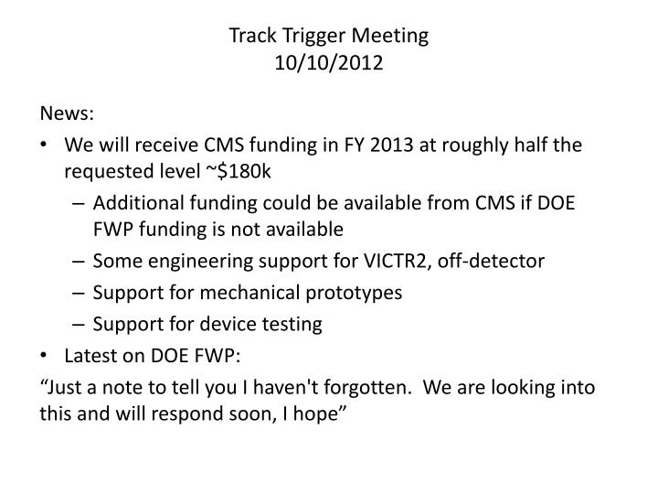
Track Trigger Meeting 10/10/2012. News: We will receive CMS funding in FY 2013 at roughly half the requested level ~$180k Additional funding could be available from CMS if DOE FWP funding is not available Some engineering support for VICTR2, off-detector Support for mechanical prototypes

E N D
Track Trigger Meeting10/10/2012 News: • We will receive CMS funding in FY 2013 at roughly half the requested level ~$180k • Additional funding could be available from CMS if DOE FWP funding is not available • Some engineering support for VICTR2, off-detector • Support for mechanical prototypes • Support for device testing • Latest on DOE FWP: “Just a note to tell you I haven't forgotten. We are looking into this and will respond soon, I hope”
Other News • SVTC was an R&D fab dedicated to providing specialized wafer processing. Tezzaron was using that fab to post-process 3D wafers. • This provides a much more secure processing chain. • Provides access to a wide variety of technologies. • 18 wafers still in process at SVTC and ZiptronixfOR 3D bonding
Interconnect array Ziptronix DBI bonding array Bump bond pad 6 micron thick top silicon 4 micron pitch DBI Copperpillars
Threshold and Noise Thresholds Noise Short strips Long strips
Active Edge • Processing at VTT ... “Regarding the processing, I was hoping to be finished early next week, but just yesterday we noticed that we didn't have the contact opening (metal via) mask yet ordered. Apparently you needed to do some changes to it and we didn't make the order. Thus we are now waiting to receive the mask and finalize the process. All the wafers, 3 dummies and 6 process wafers have been planarized and they look good! I checked the planarity at the trenches on one dummy and it was 250 nm. The process wafers look better! We will check the planarity after aluminium deposition with an optical profilometer. Did you want 1 um of aluminium? We agreed to pattern aluminium on one wafer and carry some basic measurements on it - I think we should use FZ-wafer for this, ok?.” • Top tungsten plug wafer processing is almost complete at Cornell – need to test first samples for connectivity • Arranged with SLAC for final processing and singulation at the SLAC nanofabrication facility.
Active Edge • We will receive one wafer with top metal for probe testing • Test at Brown or FNAL? • They will then be “singulated” into activedie at SLAC/Stanford • Meeting at Ziptronix in mid-November to discuss details of processing. • Need top tungsten wafers by then.
Alternate 3D • The “baseline” 3D technology utilizes small fine pitch through silicon vias – they can only be bonded and thinned using a non-reworkable process therefore a large module with ~25 chips is dependent on a very high – unachievable? Yield • The active edge work is intended to address this – but it is a complex, and perhaps expensive, process. • UCD/NRL have an alternate process that we will test. • An alternative is to use a larger “via last” process and 3 layers of bump bonds. • Requires ~250 micron thick ICs • Stack thickness probably a bit larger than 1mm • Can be used with standard IC wafers • Received a quote of $68k for prototype to match active edge sensors
Silicon sensor Arloncircuit board ROIC Silicon sensor
Design Issues • Marvin’s off- detector design should deliver tracks to L1 in 1.5 microseconds • The trigger latency may (will?) be increased beyond 6.4 ms for phase 2 • The pixels should be included in a L1 trigger using a region of interest readout • There should be plenty of time • Much better z vertex resolution • Redefines the z resolution requirement for the outer tracker trigger – now a question of how large is the ROI • Can be addressed by the new task force led by Anders and Emanuelle
Status Reports • Rod Fabrication • VICTR Tests • Interposer fabrication • Module bump bonding • Off-detector design • AOB