Download
1 / 33
330 likes | 354 Views
This research introduces clock gating logic to optimize sequential circuits, reducing power consumption by gating clock signals during idle states. The paper discusses the structure, implementation, and experimental results of this novel approach.

E N D
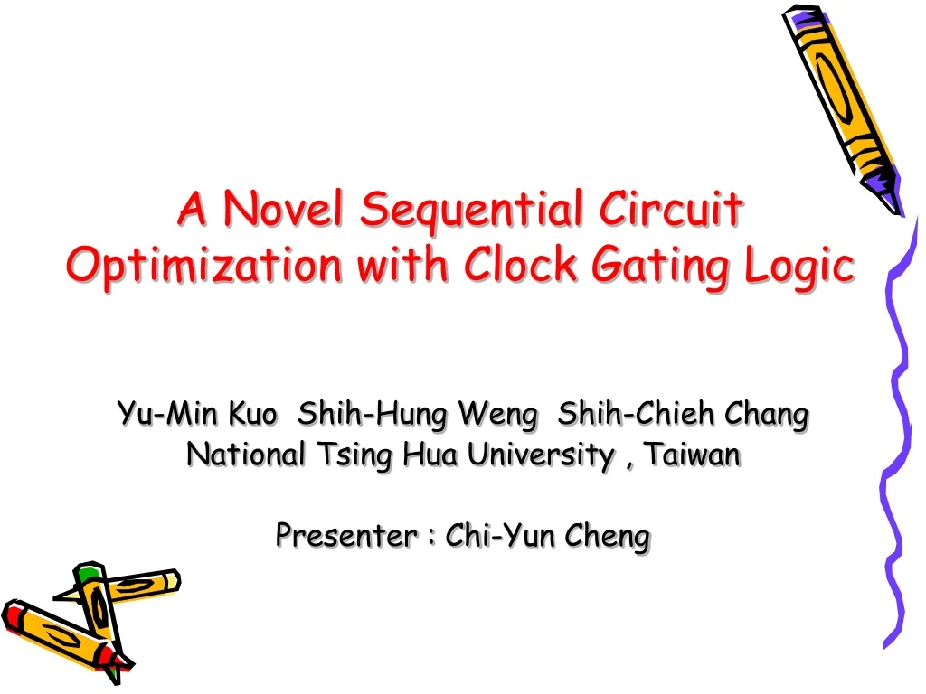
A Novel Sequential Circuit Optimization with Clock Gating Logic Yu-Min Kuo Shih-Hung Weng Shih-Chieh Chang National Tsing Hua University , Taiwan Presenter : Chi-Yun Cheng
Outline • Introduction • Logic Synthesis Using the Clock Gating Function • Experimental Results • Conclusions
Introduction Combinational elements to compute next states. Sequential elements such as Flip-Flops to store the current states. • Sequential circuit a Combinational elements FFa Input clk
Introduction • Normally, clock is delivered to all FFs periodically . • However , it is not necessary to deliver a clock pulse • to an FF in every clock cycle. • We can shut off clock signals when circuit is • in idle state or when FFs need not change their state • to save the power consumption.
Introduction Structure of the circuit ‧Next-State function to provide the next state. ‧Clock-Gating function to control the clock signal. a Next-State Function(FNS(a)) Input FFa ※ CG Cell , is used to avoid glitch . Clock-Gating Function(FCG(a)) CGC clk
Introduction ‧3-Bit Counter ‧When the clock pulse arrives , then status will be S0 → S1 → S2…… → S7 , and then return to S0 Status Current State Next State a b c an bn cn S0 0 0 0 0 0 1 S1 0 0 1 0 1 0 S2 0 1 0 0 1 1 S3 0 1 1 1 0 0 S4 1 0 0 1 0 1 S5 1 0 1 1 1 0 S6 1 1 0 1 1 1 S7 1 1 1 0 0 0
Introduction ‧When the current state (a,b,c) is (0,0,0) , the next state will be (0,0,1). The state of FFa will not change its value . Status Current State Next State a b c an bn cn S0 0 0 0 0 0 1 S1 0 0 1 0 1 1 S2 0 1 0 0 1 1 S3 0 1 1 1 0 0 S4 1 0 0 1 0 1 S5 1 0 1 1 1 0 S6 1 1 0 1 1 1 S7 1 1 1 0 0 0
Introduction • When current state (a,b,c) is equal to one of state in • S ={ (0,0,0),(0,0,1),(0,1,0),(1,0,0),(1,0,1),(1,1,0) } • the state of FFa doesn’t change. • So a clock pulse doesn’t need to arrive at FFa and can be gated. Status Current State Next State a b c an bn cn S0 0 0 0 0 0 1 S1 0 0 1 0 1 1 S2 0 1 0 0 1 1 S3 0 1 1 1 0 0 S4 1 0 0 1 0 1 S5 1 0 1 1 1 0 S6 1 1 0 1 1 1 S7 1 1 1 0 0 0 S
Introduction • Function b’+c’ can characterize current state in S . • When b’+c’ is true , no clock pulse is delivered to FF . • Can randomly assign the output of the next-state function . Status Current State Next State a b c an bn cn S0 0 0 0 0 0 1 S1 0 0 1 0 1 1 S2 0 1 0 0 1 1 S3 0 1 1 1 0 0 S4 1 0 0 1 0 1 S5 1 0 1 1 1 0 S6 1 1 0 1 1 1 S7 1 1 1 0 0 0 b’+c’
Introduction • Minimize the original next-state function ab’+ac’+a’bc a a 0 1 0 1 bc bc 00 01 11 10 00 01 11 10 use b’+c’ as don’t-care function • The result of minimization is an inverter , a’
Outline • Introduction • Logic Synthesis Using the Clock Gating Function Basic definitions and key facts The simplest implementation of FNS and FCG Heuristic minimization for FNS and FCG • Experimental Results • Conclusions
Basic definitions • a : current state value • FCG(a) : the clock-gating function of FFa • FNS(a) : the next-state function of FFa • Clock of FFa is shut off when FCG(a) is 1 a Next-State Function(FNS(a)) Input FFa Clock-Gating Function(FCG(a)) CGC clk
Two key facts • Two facts about the relationship between the next-state function (FNS) and the clock-gating function (FCG) . • Fact 1 : use FCG to optimize FNS. • Fact 2 : use FNS to optimize FCG. a Next-State Function(FNS(a)) Input FFa Clock-Gating Function(FCG(a)) CGC clk
Fact 1 • Fact 1 : When the clock is gated the next state remains the same regardless of whether the next-state function is 0 or 1 • When FCG (a) = 1 , FNS (a) = 0 or 1 (don’t-care *) a FNS(a) = * Input FFa FCG(a) = 1 CGC clk
Fact 2 • Fact 2 : When the next state and the current state value are the same , the FF remains its value regardless of whether the clock is gated or not. • When (a ≡ FNS (a)) = 1 , FCG (a) = 0 or 1 (don’t-care *) “≡ ” is XNOR a FNS(a) Input FFa The same FCG(a) = * CGC clk
Summaries • Fact1:When FCG =1 , FNS = 0 or 1. → When the clock is gated , next state can be 0 or 1. • On-set of FCG is the don’t-care set for FNS . → Can optimize FNS. • Fact2:When (a≡ FNS)=1 , FCG = 0 or 1. → When next and current state are the same, the clock can be gated or not. • On-set of (a≡ FNS) is the don’t-care set for FCG . → Can optimize FCG.
Outline • Introduction • Logic Synthesis Using the Clock Gating Function Basic definitions and key facts The simplest implementation of FNS and FCG Heuristic minimization for FNS and FCG • Experimental Results • Conclusions
Simplest implementation • We can use don’t-care conditions in Fact 1 and Fact 2 to minimize FNS and FCG. • In the following will discuss the simplest implementation of FNS and FCG.
Simplest implementation for FNS • Simplest FCG is 0 (FCG = 0) Because there exists a legal solution that the clock is not gated at all. Status Current State Next State a b c an bn cn a = an Clock can be gated, FCG = 1 S0 0 0 0 0 0 1 S1 0 0 1 0 1 1 S2 0 1 0 0 1 1 S3 0 1 1 1 0 0 S4 1 0 0 1 0 1 S5 1 0 1 1 1 0 S6 1 1 0 1 1 1 S7 1 1 1 0 0 0 a ≠ an Clock is not gated, FCG = 0
Simplest implementation for FCG • Simplest FNS is an inverter (FNS = a’) Because the clock arrives only when the FF changes its state , an inverter is used to reverse the state. Status Current State Next State a b c an bn cn S0 0 0 0 0 0 1 S1 0 0 1 0 1 1 S2 0 1 0 0 1 1 S3 0 1 1 1 0 0 S4 1 0 0 1 0 1 S5 1 0 1 1 1 0 S6 1 1 0 1 1 1 S7 1 1 1 0 0 0 a ≠ an , so the clock arrives. And an = a’ , so FNS is just an inverter
Simplest implementation • Simplest FCG is 0 (FCG = 0) • Simplest FNS is an inverter (FNS = a’) a FFa FNS(a) Input 0 CGC clk a FFa Input FCG(a) CGC clk
Implementation and Flexibility • But if the simplest implementation for one of them is chosen , there will be no flexibility for the other. • For example: FACT1:When FCG = 1 , FNS = 0 or 1. If we choose the simplest implementation such that FCG = 0 , there is no don’t-care for FNS. FNS = FORI-NS (The function isn’t changed.) FORI-NS denote the original implementation of the next-state function without the clock gating.
Outline • Introduction • Logic Synthesis Using the Clock Gating Function Basic definitions and key facts The simplest implementation of FNS and FCG Heuristic minimization for FNS and FCG • Experimental Results • Conclusions
Heuristic minimization • In traditional design flow, we always choose the simplest implementation of FCG =0 It causes that no any don’t-care for the next-state function FNS. • Explore other alternatives of implementations for FNS and FCG. • FNS and FCG are correlated. Choosing one implementation may affect the don’t-care set of the other.
Heuristic minimization • Use iterative approach to simplify both functions • Fact1:on-set of FCG(a) is don’t-care set for FNS(a). FNS*(a) ← {on-set = FNS(a) , dc-set = FCG(a)} • Fact2:on-set of (a≡ FNS(a)) is don’t-care set for FCG(a). FCG*(a) ← {on-set = FCG(a) , dc-set = (a≡ FNS(a))} • FNS*(a) and FCG*(a) is the simplified next-state function and clock-gating function
Heuristic minimization FNS*(a) <= {on-set = FNS(a) , dc-set = FCG(a)} {on-set = FCG(a) , dc-set = (a≡ FNS(a))}
Heuristic minimization FNS*(a) <= {on-set = FNS(a) , dc-set = FCG(a)} FCG*(a) <= {on-set = FCG(a) , dc-set = (a≡ FNS*(a))}
Heuristic minimization FNS*(a) <= {on-set = FNS(a) , dc-set = FCG(a)} FCG*(a) <= {on-set = FCG(a) , dc-set = (a≡ FNS*(a))} • Use these equations for iterative simplification
Outline • Introduction • Logic Synthesis Using the Clock Gating Function • Experimental Results • Conclusions
Outline • Introduction • Logic Synthesis Using the Clock Gating Function • Experimental Results • Conclusions
Conclusions • Propose the flexibility provided by the concept of the clock gating • Present facts and efficient heuristics to optimize a sequential circuit • On average , the timing of sequential circuits can be reduced about 13.99%