Download
1 / 12
120 likes | 270 Views
Tests Front-end Status. Necessity of Test board Test board architecture Time adjustement with delay chip and Input/Output (LEMO) Analog Front-end mezzanine FPGAs and interfaces Clock tree Test board power supply Test board layout status Test board pending question Analog mezzanine …

E N D
Tests Front-end Status Necessity of Test board Test board architecture Time adjustement with delay chip and Input/Output (LEMO) Analog Front-end mezzanine FPGAs and interfaces Clock tree Test board power supply Test board layout status Test board pending question Analog mezzanine … Schedule LHCb upgrade meeting
Necessity of Test board • If we want to used a A3P family, it is necessary to test many major characteristics of this components • SSO : It is imperative to measure this effect on this new family, because if it problem is important it requires major modification on the design of the board • I/O configurations / bank • There are a lot of possible standards, but generally a single one per bank • Maximum speed of specific function for data compression • On the CROC board with the ProAsics Plus family we had a lot of timing problem. We must check this part with the A3P family • With this board we will test time adjustment with Delay chip • This test board will do the readout for several analog mezzanines (based on delay line and switch methods) LHCb upgrade meeting
Tests board architecture CROC prototype tests : schedule Schedule for SPECS development Time adjustement and input/output of the board Analog Front-end mezzanine FPGA and Interfaces LHCb upgrade meeting
Time adjustement with delay chip and Input/Output (LEMO) CROC prototype tests : schedule Schedule for SPECS development More information on the clock tree slide ! • 2 Inputs (NIM translator) for each FPGA • 2 Output (NIM translator) for each FPGA • 1 Input Ext_Clk (NIM translator) for A3PE • 1 Output Ext_Clk (NIM translator) for A3PE LHCb upgrade meeting
Analog Front-end mezzanine CROC prototype tests : schedule Schedule for SPECS development • 8 x {ADC_Data Channel (12b)} • 8 x {Clk for ADC_Data Channel (LVDS)} • 2 x Global Clk (LVDS) • 4 Spare for A3PE • 4 Spare for AX500 • I2C • Reset LHCb upgrade meeting
FPGA and Interfaces CROC prototype tests : schedule Schedule for SPECS development FPGA and Interfaces • A3PE1500 • AX500 (socket) • SPECS and USB Interface through A3PE • I2C Interface from A3PE to AX • JTAG download for A3PE • JTAG for AX : Silicon Explorer LHCb upgrade meeting
Tests board power supply CROC prototype tests : schedule Schedule for SPECS development P7V Regulator - 4913 AVCC for Analog Mezza (+3 to +5V) Regulator - 4913 DVDD for Analog Mezza (+2V5 to +3V3) VCC for board (+5V) Regulator - 4913 P3V3 for board (+3,3v) Regulator - 4913 (VccIO bank fixe) P1V5 for FPGA core 1,5v < VccIOB_Var < +2,5v) Regulator - 4913 (VccIO bank variable) P2V5 for bank (+2,5v) Regulator - 4913 (VccIO bank LVDS) M7V Regulator - 7913 AVEE for Analog Mezza (-3 to -5V) Regulator - 7913 VCC for board (-5V) • Lab. Power Supply input (+/- 7V) • 8 Radiation tolerance regulator ! ! LHCb upgrade meeting
Tests board Clock Tree CROC prototype tests : schedule Schedule for SPECS development • Each FPGA receive 2 adjustable Clock (LVDS) • Analog mezzanine receive also 2 adjustable Clock (LVDS) • Each ADC_Channel receive 1 Clock (LVDS) LHCb upgrade meeting
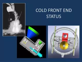
Test board layout status IN / OUT (NIM) Delay Chip USB A3PE1500 Top SPEC Mezzanine AX500 Bottom Analog Mezzanine 120x120mm REGULATOR IN / OUT (NIM) LHCb upgrade meeting
Test board layout status (2) LHCb upgrade meeting
Pending question • Analog mezzanine Request implemented, last chance for modification !! • Size of the board ? • Position of the connectors ? • Pinout modification of the connectors ? (distribution of GND pins) • Others questions ? Analog Mezzanine 98 mm 95 mm LHCb upgrade meeting
Tests board schedule CROC prototype tests : schedule Schedule for SPECS development December January February End of Schematic Holiday CAD Manufacturing Tests LHCb upgrade meeting