Download
1 / 62
620 likes | 665 Views
This guide explores building a TOY Machine processor, detailing the major components like ALU, memory, registers, and program counter. It delves into determining datapath requirements, flow of bits, and analyzing how to implement instructions with control signals settings.

E N D
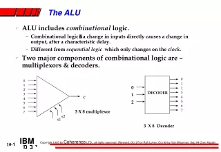
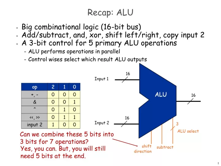
Can we combine these 5 bits into 3 bits for 7 operations? Recap: ALU • Big combinational logic (16-bit bus) • Add/subtract, and, xor, shift left/right, copy input 2 • A 3-bit control for 5 primary ALU operations • ALU performs operations in parallel • Control wises select which result ALU outputs Yes, you can. But, you will still need 5 bits at the end.
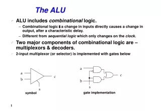
Recap: Multiplexer Goal: select from one of n k-bit buses • Implemented by layering k n-to-1 multiplexer
Clock • Clock. • Fundamental abstraction: regular on-off pulse. • on: fetch phase • off: execute phase • External analog device. • Synchronizes operations of different circuit elements. • Requirement: clock cycle longer than max switching time. cycle time on Clock off
Fetch Execute The TOY Machine • Combinational circuits. ALU. • Sequential circuits. Memory. • Machine architecture. Wire components together to make computer. • TOY machine. • 256 16-bit words of memory. • 16 16-bit registers. • 1 8-bit program counter. • 16 instruction types.
Design a processor • How to build a processor • Develop instruction set architecture (ISA) • 16-bit words, 16 TOY machine instructions • Determine major components • ALU, memory, registers, program counter • Determine datapath requirements • Flow of bits • Analyze how to implement each instruction • Determine settings of control signals
Instructions Instructions 0: halt 8: load 1: add 9: store 2: subtract A: load indirect 3: and B: store indirect 4: xor C: branch zero 5: shift left D: branch positive 6: shift right E: jump register 7: load address F: jump and link Build a TOY: Interface Instruction set architecture (ISA). • 16-bit words, 256 words of memory, 16 registers. • Determine set of primitive instructions. • too narrow cumbersome to program • too broad cumbersome to build hardware • 16 instructions.
TOY Reference Card 15 14 13 12 11 10 9 8 7 6 5 4 6 3 2 1 0 Format 1 opcode dest d source s source t Format 2 opcode dest d addr # Operation Fmt Pseudocode 0: halt 1 exit(0) 1: add 1 R[d] R[s] + R[t] 2: subtract 1 R[d] R[s] - R[t] 3: and 1 R[d] R[s] & R[t] Register 0 always 0.Loads from mem[FF] from stdin.Stores to mem[FF] to stdout. 4: xor 1 R[d] R[s] ^ R[t] 5: shift left 1 R[d] R[s] << R[t] 6: shift right 1 R[d] R[s] >> R[t] 7: load addr 2 R[d] addr 8: load 2 R[d] mem[addr] 9: store 2 mem[addr] R[d] A: load indirect 1 R[d] mem[R[t]] B: store indirect 1 mem[R[t]] R[d] C: branch zero 2 if (R[d] == 0) pc addr D: branch positive 2 if (R[d] > 0) pc addr E: jump register 1 pc R[t] F: jump and link 2 R[d] pc; pc addr
Design a processor • How to build a processor • Develop instruction set architecture (ISA) • 16-bit words, 16 TOY machine instructions • Determine major components • ALU, memory, registers, program counter • Determine datapath requirements • Flow of bits • Analyze how to implement each instruction • Determine settings of control signals
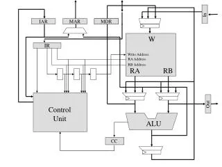
Cond Eval Registers W Data Memory A Data A L U IR Addr op B Data W Addr d R Data A Addr s B Addr W Data t W W Components PC + 1 Clock
Cond. Eval. X0 : Y0 Y0 =0 X15 16 Cond Eval X Y1 Y1 >0
Design a processor • How to build a processor • Develop instruction set architecture (ISA) • 16-bit words, 16 TOY machine instructions • Determine major components • ALU, memory, registers, program counter • Determine datapath requirements • Flow of bits • Analyze how to implement each instruction • Determine settings of control signals
Cond Eval Registers W Data Memory A Data A L U IR Addr op B Data W Addr d R Data A Addr s B Addr W Data t W W Datapath PC + 1 8 7 1-6 R[d] addr R[d] mem[addr] R[d] R[s] ALU R[t] 9 A B R[d] mem[R[t]] mem[addr] R[d] mem[R[t]] R[d] CD E F pc R[t] if (R[d]?) pc addr R[d] pc; pc addr
Cond Eval Registers W Data Memory A Data A L U IR Addr op B Data W Addr d R Data A Addr s B Addr W Data t W W Datapath 16 8 result of ALU or address for load address pc for jump and branch address for load/store 0 8 pc for jal load PC + 16 1 0 8 addr 8 store data pc+1
Design a processor • How to build a processor • Develop instruction set architecture (ISA) • 16-bit words, 16 TOY machine instructions • Determine major components • ALU, memory, registers, program counter • Determine datapath requirements • Flow of bits • Analyze how to implement each instruction • Determine settings of control signals
Cond Eval Registers 10 01 00 W Data Memory A Data A L U IR 1 0 Addr 0 1 1 0 op B Data W Addr d R Data 1 0 A Addr s B Addr W Data t W W Datapath PC + 1
Cond Eval Registers 10 01 00 W Data Memory A Data A L U IR 1 0 Addr 0 1 1 0 op B Data W Addr d R Data 1 0 A Addr s B Addr W Data t W W Control 2 PC WRITE_REG MUX 5 MEM_ADDR MUX ALU_OP PC_MUX ALU MUX WRITE_PC + 1 READ_REG A MUX WRITE_IR WRITE_REG WRITE_MEM CLOCK_MEM CLOCK_REG A total of 17 control signals
Cond Eval Registers 10 01 00 W Data Memory A Data A L U IR 1 0 Addr 0 1 1 0 op B Data W Addr d R Data 1 0 A Addr s B Addr W Data t W W Control TOY architecture =0 >0 2 PC 4 5 + 1 Opcode 1-bit counter Execute Fetch Clock Clock
Cond Eval Registers 10 01 00 W Data Memory A Data A L U IR 1 0 Addr 0 1 1 0 op B Data W Addr d R Data 1 0 A Addr s B Addr W Data t W W Control Clock =0 >0 2 PC 4 5 + 1 Opcode 1-bit counter Execute Fetch Clock Clock
1-bit counter • 1-bit counter • Circuit that oscillates between 1 and 0.
Clock • Two cycle design (fetch and execute) • Use 1-bit counter to distinguish between 2 cycles. • Use two cycles since fetch and execute phases each access memory and alter program counter.
Phase 4 execute & clock Phase 2 fetch & clock Phase 1 fetch Phase 3 execute Clocking Methodology • Two-cycle design. • Each control signal is in one of four epochs. • fetch [set memory address from pc] • fetch and clock [write instruction to IR] • execute [set ALU inputs from registers] • execute and clock [write result of ALU to registers] Fetch Fetch Execute Clock
Cond Eval Registers 10 01 00 W Data Memory A Data A L U IR 1 0 Addr 0 1 1 0 op B Data W Addr d R Data 1 0 A Addr s B Addr W Data t W W execute fetch Clocking Methodology 2 PC 5 + 1
Cond Eval Registers 10 01 00 W Data Memory A Data A L U IR 1 0 Addr 0 1 1 0 op B Data W Addr d R Data 1 0 A Addr s B Addr W Data t W W Example: ADD 20 ???? 2 PC 5 + 1 PC=20 Mem[20]=1234 R[3]=0028 R[4]=0064
Cond Eval Registers 10 01 00 W Data Memory A Data A L U IR 1 0 Addr 0 1 1 0 op B Data W Addr d R Data 1 0 A Addr s B Addr W Data t W W Example: ADD (fetch) 20 ???? 2 PC 20 5 + 1 PC=20 Mem[20]=1234 R[3]=0028 R[4]=0064
Cond Eval Registers 10 01 00 W Data Memory A Data A L U IR 1 0 Addr 0 1 1 0 op B Data W Addr d R Data 1 0 A Addr s B Addr W Data t W W Example: ADD (fetch) 20 ???? 2 PC 20 5 1234 + 1 PC=20 Mem[20]=1234 R[3]=0028 R[4]=0064
Cond Eval Registers 10 01 00 W Data Memory A Data A L U IR 1 0 Addr 0 1 1 0 op B Data W Addr d R Data 1 0 A Addr s B Addr W Data t W W Example: ADD (fetch) 20 ???? 2 PC 20 5 21 1234 + 1 21 PC=20 Mem[20]=1234 R[3]=0028 R[4]=0064
Cond Eval Registers 10 01 00 W Data Memory A Data A L U IR 1 0 Addr 0 1 1 0 op B Data W Addr d R Data 1 0 A Addr s B Addr W Data t W W Example: ADD (fetch and clock) 21 1234 2 PC 1 5 21 2 3 + 4 1 PC=21 IR=1234 Mem[20]=1234 R[3]=0028 R[4]=0064
Cond Eval Registers 10 01 00 W Data Memory A Data A L U IR 1 0 Addr 0 1 1 0 op B Data W Addr d R Data 1 0 A Addr s B Addr W Data t W W Example: ADD (execute) 21 1234 2 PC 1 5 2 3 3 + 4 4 1 PC=21 IR=1234 Mem[20]=1234 R[3]=0028 R[4]=0064
Cond Eval Registers 10 01 00 W Data Memory A Data A L U IR 1 0 Addr 0 1 1 0 op B Data W Addr d R Data 1 0 A Addr s B Addr W Data t W W Example: ADD (execute) 21 1234 0028 2 PC 1 0064 5 2 3 3 + 4 4 1 PC=21 IR=1234 Mem[20]=1234 R[3]=0028 R[4]=0064
Cond Eval Registers 10 01 00 W Data Memory A Data IR 1 0 Addr 0 1 1 0 op B Data W Addr d R Data 1 0 A Addr s B Addr W Data t W W Example: ADD (execute) 008C 21 1234 0028 2 008C A L U PC 1 0064 5 2 3 3 + 4 4 1 PC=21 IR=1234 Mem[20]=1234 R[3]=0028 R[4]=0064
Cond Eval Registers 10 01 00 W Data Memory A Data IR 1 0 Addr 0 1 1 0 op B Data W Addr d R Data 1 0 A Addr s B Addr W Data t W W Example: ADD (execute and clock) 008C 21 1234 2 A L U PC 1 5 2 2 3 + 4 1 PC=21 IR=1234 R[2]=008C Mem[20]=1234 R[3]=0028 R[4]=0064
Cond Eval Registers 10 01 00 W Data Memory A Data A L U IR 1 0 Addr 0 1 1 0 op B Data W Addr d R Data 1 0 A Addr s B Addr W Data t W W Example: Jump and link 2 PC 5 + 1 PC=20 Mem[20]=FF30 R[3]=0028 R[4]=0064
Cond Eval Registers 10 01 00 W Data Memory A Data A L U IR 1 0 Addr 0 1 1 0 op B Data W Addr d R Data 1 0 A Addr s B Addr W Data t W W Control Fetch =0 >0 2 PC 4 5 + 1 Opcode 1-bit counter Execute Fetch Clock Clock
Program counter • Read program counter when • Fetch • Execute for jal • Write program counter when • Fetch and clock • Execute and clock depending on conditions
Cond Eval Registers 10 01 00 W Data Memory A Data A L U IR 1 0 Addr 0 1 1 0 op B Data W Addr d R Data 1 0 A Addr s B Addr W Data t W W Control Fetch and clock =0 >0 2 PC 4 5 + 1 Opcode 1-bit counter Execute Fetch Clock Clock
Cond Eval Registers W Data Memory A Data A L U IR Addr op B Data W Addr d R Data A Addr s B Addr W Data t W W Control Execute =0 >0 2 PC 4 5 + 1 Opcode 1-bit counter Execute Fetch Clock Clock
17 control signals 17 control signals … … Control Control • Two approaches to implement control • Micro-programming • Use a memory (ROM) for micro-code • More flexible • Easier to program • Hard-wired • Use logic gates and wire • More efficient 512x17 ROM 9-bit address : : >0 =0 Opcode Execute Fetch Clock
Control ALU MUX
Cond Eval Registers 10 01 00 W Data Memory A Data A L U IR 1 0 Addr 0 1 1 0 op B Data W Addr d R Data 1 0 A Addr s B Addr W Data t W W Control Execute and clock (write-back) =0 >0 2 PC 4 5 + 1 Opcode 1-bit counter Execute Fetch Clock Clock