Download
1 / 17
180 likes | 313 Views
Interfacing a microprocessor-based system to the real world. Analog and digital signals The bridge: Sampling Theorem Conversion concepts Conversion circuitry. Analog to Digital (and back again). Analog Signals. x(t). continuous range. time. The real world is analog.

E N D
Interfacing a microprocessor-based system to the real world. • Analog and digital signals • The bridge: Sampling Theorem • Conversion concepts • Conversion circuitry Analog to Digital (and back again)
Analog Signals x(t) continuous range time • The real world is analog. • Signals vary continuously with time. • Analog signals take arbitrarily many values. • Examples: • audio signal from microphone or cassette player • video signal from VCR or video camera • x/y voltage outputs from joystick
Digital Signals v6 v5 v4 x(t) v3 v2 v1 time • The microprocessor world is digital. • Limited number of separate (discrete) values at each time step. • Digital signals take only these values, nothing inbetween. • Computers: Two values (0 or 1) corresponding to low/high value of electrical property (usually voltage). • In general: 2n values (n-bit representation).
Analog vs. Digital • To compute on a Microprocessor, we need a digital value. • And by “compute”, we mean: • making decisions based on signals • combining multiple signals together • analyze the signal for a data transmission • generate a modification of the signal
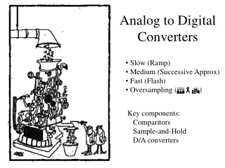
Signal Conversion • To interface microprocessors to real-world (analog) systems, we need converters. • Digital to Analog Converters (DAC): Convert a digital input (e.g. binary word) to analog output (e.g. current or voltage). • Analog to Digital Converters (ADC): Convert an analog input to digital output. analog digital electrical mechanical electrical ADC mic mP DAC mechanical electrical electrical speaker
Analog to Digital Conversion • Ideal 2-bit ADC • Input range: Analog voltage between 0 and Vmax • Output: 2-bit code Vmax analog input voltage ¾ Vmax ½ Vmax ¼ Vmax 0 00 01 10 11 digital output
Conversion of Signals over Time Sample and hold n-bit ADC n analog analog digital • Must hold input signal while converting. • “Sample and hold” circuit takes in (samples) analog value and holds it still while A to D conversion is taking place. • What is the minimum rate S at which the analog input should be sampled? • Minimum sampling rate S determines the minimum acceptable speed of A to D conversion.
Sampling • Sampling rate must be high enough so that “no information is lost”. • What is the information of a signal?
Sampling Theorem Harmonic analysis Signals can be expressed as weighted sums of harmonic functions. Shannon’s Theorem (Nyquist Sampling Theorem) To sample a bandlimited signal x(t) with no loss of information, the sampling rate must be at least twice the frequency of the highest frequency component. Example: Audio signals typically include components up to 20KHz. CDs sample at 44.1KHz. DATs sample at 32, 44.1, or 48KHz.
Basic Converter Characteristics • Resolution: Fraction of analog range as defined by the number of bits on the digital side of the converter. • An n-bit ADC divides analog voltage range [0 , Vmax] into _____ sections and its resolution is _____ of Vmax. • Error: Difference between analog value you believe a digital value represents and what that analog value actually is. • Even ideal converters introduce some error.
Quantization Error Vmax ¾ Vmax analog input quantization error ½ Vmax ¼ Vmax 0 00 01 10 11 • Inherent in converting continuous values to a finite number of discrete values. • Every voltage in the range [1/2 Vmax , ¾ Vmax) is mapped to “10”. • To minimize worst-case error, we assume that “10” means _____ Vmax. • Worst-case error is __________ . • For normalization, quantization error is expressed in terms of the ideal analog difference represented by a unit change in the digital value, referred to as LSB. • Quantization error is always equal to +/- ½ LSB.
ADC #1: Flash Vref Vin priority encoder R + _ 3 R + _ 2 2 Dout R + _ 1 R Vcc 0
ADC #2: Single-Slope Integration Vin done + _ Vcc I C EN* n-bit counter CLK • Start: Reset counter, discharge C. • Charge C at fixed current I until Vc > Vin . How should C, I, n, and CLK be related? • Final counter value is Dout. • Conversion may take several milliseconds.
ADC #3: Successive Approximation (1/2) Vref DAC Dout n control successive approximation register + _ Vin CLK • Binary search to match input voltage. • Conversion time > n times DAC settling time. • Input should stay stable throughout conversion.
Successive Approximation Algorithm • Binary search algorithm • Set successive approximation register to 0 • For each bit from MSB to LSB do • flip bit to 1 • if DAC output > Vin , reset bit to 0 Example Vref = 15V , Vin = 10V , 4 bits , binary code = voltage value iteration DAC out comparison A3A2A1A0
DAC #1: Voltage Divider Din Vref 2 2-to-4 decoder R R Vout R R
DAC #2: R/2R Ladder Vref R R R 2R 2R 2R 2R 2R Iout D3 (MSB) D2 D1 D0 (LSB)