Download
1 / 18
180 likes | 323 Views
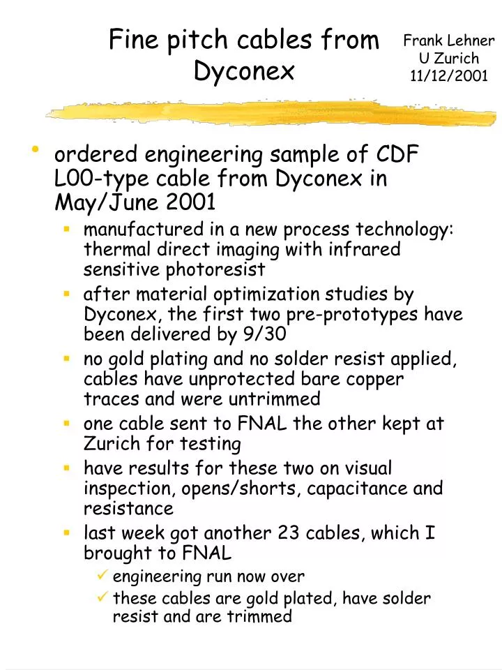
Fine pitch cables from Dyconex. Frank Lehner U Zurich 11/12/2001. ordered engineering sample of CDF L00-type cable from Dyconex in May/June 2001 manufactured in a new process technology: thermal direct imaging with infrared sensitive photoresist

E N D
Fine pitch cables from Dyconex Frank Lehner U Zurich 11/12/2001 • ordered engineering sample of CDF L00-type cable from Dyconex in May/June 2001 • manufactured in a new process technology: thermal direct imaging with infrared sensitive photoresist • after material optimization studies by Dyconex, the first two pre-prototypes have been delivered by 9/30 • no gold plating and no solder resist applied, cables have unprotected bare copper traces and were untrimmed • one cable sent to FNAL the other kept at Zurich for testing • have results for these two on visual inspection, opens/shorts, capacitance and resistance • last week got another 23 cables, which I brought to FNAL • engineering run now over • these cables are gold plated, have solder resist and are trimmed
Status of fine pitch flex from Dyconex • schematics of the cable (L00): • 128 channels/traces • 13.7 cm of 50mm pitch traces • 26.0 cm of 100mm pitch traces • fan-in and fan-out region (1.7-2.9 cm) • total trace length including fan-in/out between 41.4 – 42.6 cm • 2 rows of bond pads on each side • two traces for bias lines • general • Dyconex tried to minimize trace width (lower capacitance) • trace width measured typically to 7-8 mm
Status of fine pitch flex from Dyconex • bond pad regions: • outer pads are big enough, size is ~50 mm x 210 mm • pads of inner row region very small, only ~30 mm x 190 mm • Dyconex can try to increase pad size, but not by much. Difficult, since distance pad-trace becomes ~20um • bond tests necessary to see if we can wire bond on such small pads • two different kind of platings on pads on the 23 new cables: only gold and nickel+gold outer inner
Status of fine pitch flex from Dyconex • performed optical inspection and electrical measurement on first flex cable • total of 3 open traces visually found • not so bad for first shot! • opens confirmed by trace continuity measurements • no shorted traces detected, only few regions with slight metal excess open trace excess metal – no short
Status of fine pitch flex from Dyconex • Other typical problems: • regular and systematic trace offset by ~5 mm every 2 mm (just a shift of one pixel size during imaging) • inherent to imaging process and fixed only by a new plotter (a purchase is planned in one year from now)
Status of fine pitch flex from Dyconex • in fan-in/out regions, critical thinning of traces along the horizontal axis observed • trace width should be increased in fan-in/out region
Status of fine pitch flex from Dyconex • spots of adhesive on few traces • looks serious, but not harmful – better cleaning/rinsing will be done for further flexes
fine pitch flex cable from Dyconex • Capacitance measurements • LCR four probe measurement • measure capacitance of one trace against all others (total capacitance seen by one trace) At 1 MHz: C~15.3 pF for 42cm => 0.36pF/cm At frequencies above 1MHz capacitance measurement inaccurate due to cable inductance. Result confirmed by Kazu’s measurements at FNAL with 2nd cable
fine pitch flex from Dyconex • Capacitance of one trace to the left and right neighbors has been determined to be 12 pF only,i.e. 0.28 pF/cm • next-to-next neighbors carry 20% of the total capacitance • the 0.28 pF/cm is in fair agreement with analytical calculation (~0.23pF/cm):
fine pitch flex from Dyconex • the capacitance will be higher if solder resist (coating) is applied • calculations show an 20% increase for 2mm coating • expect for the new 23 cables higher capacitances • need also to disentangle experimentally the part of the capacitance with 50mm and 100mm pitch • noise contribution: • assume SVX4: 450+43*C_tot and 1.2pF/cm for Si • C_tot=C_Si+C_flex~37pF (for 42cm cable) • noise~2040e • acceptable
Status of fine pitch flex from Dyconex • trace resistance as measured by H. Haggerty R~200-220 W or 4.7-5.2 W/cm • expect ~4.3-4.9 W/cm from copper resistance and trace widths and thickness
Status of fine pitch flex from Dyconex • serial noise due to Rs: ENC=13*C_tot*(Rs/t) • Rs=Rs_Si+Rs_flex • Rs_Si specified to be less than 30W/cm • Rs=500-520 W • serial noise ~950e • However: conservative noise assumption • total noise: 2250e • wider traces would decrease Rs but enlarge capacitance => stay with thin traces
shielding • CDF experience shows that shielding of cable is mandatory to avoid noise pick up • ground layer will also reduce cross talk induced by inductive coupling • for L0, cables will run in a stack of up to 12 single flex cables • stacked cables also exhibit capacitances to each other => have to separate cables • however: space constrains are tight • maximum 4.6 mm space left before we hit outer sensors • subtract 1 mm clearance for wirebonds • stacked cable area: 3.6mm left, meaning ~200mm in between cables • how ‘flat’ can we stack flex cables? Have to allow for tolerances, bends, warps in the cables • individual shield: • sandwich the single cable by a 80 mm thick low-e material (foam) underneath the cable and add a mesh copper layer with copper laminated Kapton • copper layer can be used for individual +HV supply • extremely difficult to make individual shields under such tight space constrains • common shielding: • wrap stack into a copper foil • Guard trace: add additional guard traces on flex
shielding • additional GND layer under the Kapton flex will increase capacitances seen by one trace • shown is a calculation for two er for a CPW (w/o GND layer) and a CPWCB (w/ GND layer) • Capacitance to GND layer not important for heights>200mm (100mm) if er=3.5 (1.5)
Repair on cables • it is unlikely to get zero fault cables • accept cables with 1-2 faults, either opens or shorts • repair on painted (i.e. having solder resist) cable is time consuming. CDF has done it though • bonding the traces (~7um wide) in case of opens is extremely difficult: • need very thin wire ~<10um • ETH Zurich has some experience with ultra-thin wires (AMS) • however: bonding on copper difficult • propose two pairs of spare traces at left and right border of cable • open or shorted traces can then conveniently skipped
How to proceed with fine pitch flex from Dyconex • from prototypes to preproduction: • Dyconex would have more process parameters to tune in order to improve the quality of the cable • engineering run is over and ‘the remaining 10%’ are making the effort as the Dyconex engineer says • especially gold plating is not yet optimized • several problems related to plating process • bonding is an important issue • preliminary price tag for a mass production: $409/pc with one allowed bad trace • have to go with at least another prototype sample as soon as we have our own cable layout • Dyconex is moving their plant to outside the city limit of Zurich (still relatively close too my place) • they expect to be back in operation by February 2002
other games to play • try to go with a 25mm thick Kapton cable => will reduce the capacitance • plasma etch Kapton material between copper traces in order to make grooves into the cable => lower capacitance • use another dielectric substrate than standard Kapton • add halogens? • polyethylene or similar. Has lower dielectric constant. However, radiation hardness not really good • Liquid polymer – too fancy
Conclusion: fine pitch flex from Dyconex • we have received flexes from Dyconex which are extraordinary difficult to make • these cables have been engineered in a rather short time (June – October) and using a new technique • I think Dyconex is close to demonstrate us that they are able to do such cables – but we should wait upon the result of the 23 cables • image transfer works • copper etching works • gold plating still a problem • for further improvements on cables and if we want to go with Dyconex we should make another prototype run • before we can launch this prototype run in February or March we need to converge on the design