Download
1 / 30
300 likes | 336 Views
Explore strategies to enhance current density in InP DHBTs, addressing thermal resistance and power generation for efficient high-speed operation.

E N D
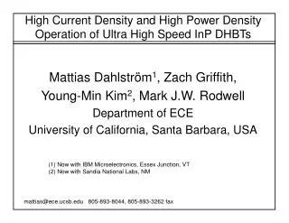
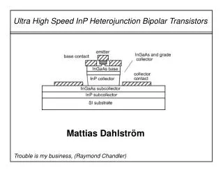
High Current Density and High Power Density Operation of Ultra High Speed InP DHBTs Mattias Dahlström1, Zach Griffith, Young-Min Kim2, Mark J.W. Rodwell Department of ECE University of California, Santa Barbara, USA (1) Now with IBM Microelectronics, Essex Junction, VT (2) Now with Sandia National Labs, NM mattias@ece.ucsb.edu 805-893-8044, 805-893-3262 fax
Overview • Fast devices and circuits need high current! • Current limited by • Kirk current threshold • Device heating • Thermal resistance Device heating • Design of low thermal resistance HBT • High Current Devices with state of the art RF performance
The need for high current density Scaling laws: Single HBT: ft Je=8 mA/mm2 Digital circuit Key performance parameters: Je=6.9 mA/mm2 Minimize capacitance charging times! Increase current density Output spectrum @ 59.35 GHz, fclk=118.70 GHz
Thermal conductivity of common materials Ternaries lattice matched to InP
Vbe = 0.95 V, Vce= 1.3 V HBT: Where is the heat generated? Power generation: JE x VCE=6 x 1.5 V=9 mW/mm2 In the intrinsic collector
HBT: heat transport Thermal resistance of materials in collector and subcollector critical Main heat transport is through the subcollector to the substrate Up to 30 % heat transport up through the emitter contact
How to design a low thermal resistance HBT A five step process Identify high thermal resistance materials change them low thermal resistance materials Very simple!
SHBT: InGaAs collector Design of low thermal resistance HBT: Initial design: InGaAs collector
SHBT: InGaAs collector, InP emitter Design of low thermal resistance HBT: Emitter: InAlAsInP
DHBT: InGaAs/InP collector Design of low thermal resistance HBT: InGaAs collector InP collector with InGaAlAs grade
DHBT: InGaAs/InP collector, InGaAs/InP subcollector Design of low thermal resistance HBT: InGaAs subcollector InGaAs/InP composite subcollector
DHBT: InGaAs/InP collector, thin InGaAs/InP subcollector Design of low thermal resistance HBT: Thick InGaAs in subcollector thin InGaAs in subcollector
Metamorphic-DHBT: InGaAs/InP collector, InGaAs/InP subcollector Young-Min Kim Design of low thermal resistance Metamorphic HBT: InAlAs,InAlP, InGaAs buffersInP buffer
Experimental Measurement of Temperature Rise Temperature rise can be calculated by measuring IC,VCE and DVBE No thermal instability as long as slope<∞ each VBE gives a unique IC
Thermoelectric feedback coefficient (data from W. Liu) W. Liu: “Thermal Coupling in 2-Finger Heterojunction Bipolar Transistors” , IEEE Transactions on Electron Devices, Vol 42 No6, June 1995 W. Liu: H-F. Chau, E. Beam, "Thermal properties and Thermal Instabilities of InP-Based Heterojunction Bipolar Transistors”, IEEE Transactions on Electron Devices, Vol 43 No3, March 1996 Thermoelectric feedback coefficient for AlGaAs/GaAs HBTs 4 % smaller Not a large influence from material or structure variations
InGaAs 3E19 Si 400 Å InP 3E19 Si 800 Å InP 8E17 Si 100 Å InP 3E17 Si 300 Å InGaAs 8E19 5E19 C 300 Å Setback 3E16 Si 200 Å Grade 3E16 Si 240 Å InP 3E18 Si 30 Å InP 3E16 Si 1030Å InP 1.5E19 Si 500 Å InGaAs 2E19 Si 125Å InP 3E19 Si 3000Å SI-InP substrate High f DHBT Layer Structure and Band Diagram Vbe = 0.75 V, Vce= 1.3 V Emitter Collector Base • Compared to previous UCSB mesa HBT results: • Thinner InP collector—decrease c • Collector doping increased—increase JKirk • Thinner InGaAs in subcollector—remove heat • Thicker InP subcollector—decrease Rc,sheet
Thermal resistance results: lattice matched 25 nm InGaAs Measured thermal resistances for lattice matched HBTs. Ic= 5 mA, Vce=1.5 V, P=7.5 mW 12.5 nm InGaAs 50 nm InGaAs 25 nm InGaAs: large improvement
Thermal resistance results: metamorphic 50 nm InGaAs InAlP buffer Measured thermal resistances for metamorphic HBTs. Ic= 5 mA, Vce=1.5 V, P=7.5 mW 25 nm InGaAs InP buffer InAlP InP buffer: large improvement 50 nm InGaAs 25 nm InGaAs: small improvement
Device and circuit results Zach Griffith Transistor operation at 13 mA/mm2 150 nm InGaAs/InP collector 28 transistor static frequency divider @ fclk=118.7 GHz shown To be reported, 150 GHz static divider using same Type 1 DHBT structure—chirped superlattice Continuous operation at high current densities greater than peak rf performance (Je = 8 mA/m2) 370 GHz ft at Jc>8 mA/mm2
Our Mesa DHBTs have Safe Operating AreaExtending beyond High-Speed Logic Bias Conditions Low-current breakdown is > 6 Volts this has little bearing on circuit design Safe operating area is > 10 mW/um2 these HBTs can be biased ....at ECL voltages ...while carrying the high current densities needed for high speed
Conclusions • DHBT design with InP subcollector • very low thermal resistance • Metamorphic DHBT with InP buffer • low thermal resistance • DHBT operation at Jc>13 mA/mm2 • Optimal device and circuit performance at Jc up to 8 mA/mm2 • HBT I-V operating area allows static frequency dividers operating at speeds over 150 GHz
Why is thermal management important? • As J increases so does the power density. This will lead to an increase in the temperature. For VCE=1V PD=10.6mWμm-3 For VCE=1V PD=98mWμm-3!!
Thermal Modeling of HBT (1) • 3D Finite Element using Ansys 5.7 • K (Thermal conductivity) depends temperature • K depends on doping • For GaAs heavily doped GaAs 65% less than undoped GaAs • Unknown for InP or InGaAs use GaAs dependency Large uncertainty in values J.C.Brice in “Properties of Indium phosphide” eds S Adachi and J.Brice pubs INSPEC London p20-21 S Adachi in “Properties of Latticed –Matched and strained Indium Gallium Arsenide” ed P Bhattacharya pubs INSPEC London p34-39 “CRC Materials science and engineering handbook”, 2nd edition ,eds J.F Shackelford,A.Alexander, and J.S Park, pubs CRC press, Boca Raton, p270
Validation of Model Ian Harrison Caused by Low K of InGaAs Max T in Collector Advice Limit InGaAs Increase size of emitter arm Ave Tj (Base-Emitter) =26.20°C Measured Tj=26°C Good agreement.
Analysis of 40,80,160 Gbit/s devices Ian Harrison • To obtain speed inprovements require to scale other device parameters. Reduction of parasitic CBC Conservative 1.5x bit rate When not switching values will double Device parameters after Rodwell et al
Mesa DHBT with 0.6 mm emitter width, 0.5 mm base contact width Z. Griffith, M Dahlström
Improved emitter heatsinking Layout improvement: Emitter heat sinking Emitter interconnect metal 2 μm to 7 μm ~30 % of heat out through emitter Negligible increase in Cbe