Download
1 / 12
270 likes | 2.02k Views
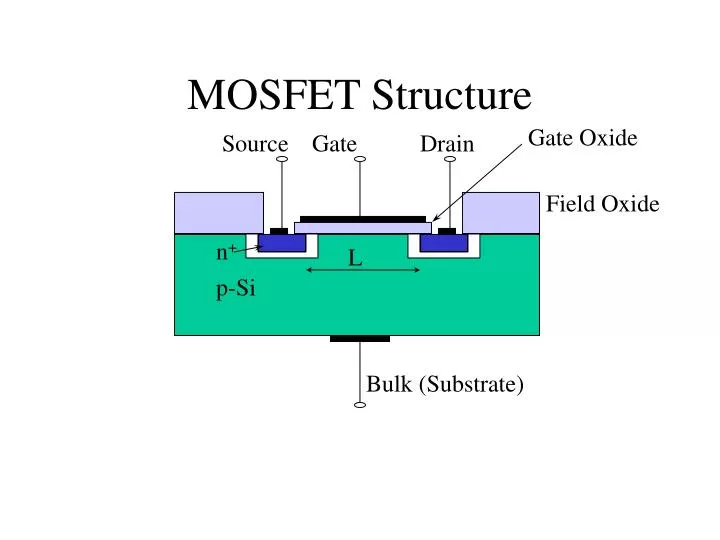
Gate Oxide. Source. Gate. Drain. Field Oxide. n +. L. p-Si. Bulk (Substrate). MOSFET Structure. Importance for LSI/VLSI Low fabrication cost Small size Low power consumption Applications Microprocessors Memories Power Devices Basic Properties Unipolar device

E N D
Gate Oxide Source Gate Drain Field Oxide n+ L p-Si Bulk (Substrate) MOSFET Structure
Importance for LSI/VLSI • Low fabrication cost • Small size • Low power consumption • Applications • Microprocessors • Memories • Power Devices • Basic Properties • Unipolar device • Very high input impedance • Capable of power gain • 3/4 terminal device, G, S, D, B • Two possible device types: enhancement mode; depletion mode • Two possible channel types: n-channel; p-channel
D D B B G G S S Symbols p Channel MOSFET n Channel MOSFET
D IDS C B A VDS Current-Voltage Characteristic
S D VG +VDS p-Si n-Channel B Channel Formation
Source Channel Drain VT VG VG-channel VDS VDS/2 Intermediate VDS(B)
S D VG +VDS p-Si n-Channel B Increased VDS
Analysis: Intermediate VDS • First Order Approximation • Gate to Channel Voltage = VGS-VDS/2 Extra term!
Source Channel Drain VG-channel VDS VG VT Pinch-off Large VDS: Saturation (C)
Analysis: Saturation (C) Pinch-off Substitute for VDS(sat) in equation for IDS to get IDS(sat)
Avalanche and Punch-Through(D) • For very large VDS, IDS increases rapidly due to drain junction avalanche. • Can give rise to parasitic bipolar action. • In short channel transistors, the drain depletion region may reach the source depletion region giving rise to ‘Punch Through’.