Download
1 / 11
120 likes | 270 Views
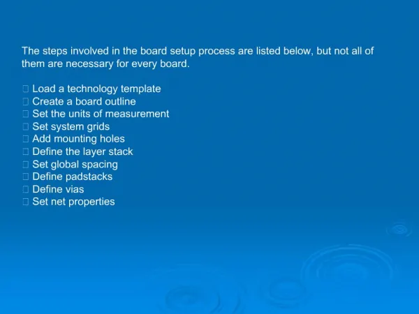
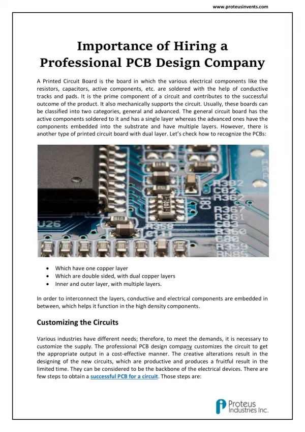
Some PCB Layout Issues. Ground Bounce. 500 mV. GND. V CCI Noise. 500 mV/DIV. V CCA Noise. 500 mV/DIV. AD Bus Signal Quality. 500 mV/DIV. V CCA /V CCI Noise Measurements. Original layout pattern for an FPGA implementing a PCI core.

E N D
Ground Bounce 500 mV GND
VCCI Noise 500 mV/DIV
VCCA Noise 500 mV/DIV
AD Bus Signal Quality 500 mV/DIV
Original layout pattern for an FPGA implementing a PCI core.
Original layout pattern for an FPGA implementing a PCI core. • Note: • Small trace width for these array power connections. • Via "islands" separating cap from FPGA