Download
1 / 14
140 likes | 148 Views
CMOS Mm-Wave Circuits and Systems for Wireless Communications<br>CMOS Mm-Wave Circuits and Systems for Wireless Communications<br>

E N D
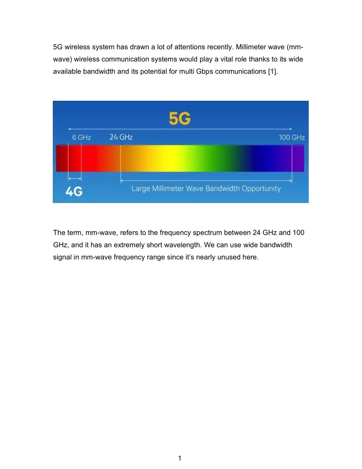
5G wireless system has drawn a lot of attentions recently. Millimeter wave (mm- wave) wireless communication systems would play a vital role thanks to its wide available bandwidth and its potential for multi Gbps communications [1]. The term, mm-wave, refers to the frequency spectrum between 24 GHz and 100 GHz, and it has an extremely short wavelength. We can use wide bandwidth signal in mm-wave frequency range since it’s nearly unused here. 1
The component carrier can have a bandwidth of 1.4, 3, 5, 10, 15 or 20 MHz, and a maximum of five component carriers can be aggregated, hence the maximum aggregated bandwidth is 100 MHz. According to Shannon theorem, as shown below: 2
Wide bandwidth can augment channel capacity. That’s why the technology, carrier aggregation, can improve data rate. Likewise, to use wideband mm-wave signal can improve data rate as well. 9 GHz bandwidth around 60 GHz [1]. The development of mm-wave technology is relevant to semiconductor process. Thanks to nanometer dimension of modern CMOS process, the transistors can achieve acceptable performance beyond 200 GHz [1]. It’s well known that the SiGe process provides more superior mm-wave performance than the CMOS process [1]. Nevertheless, higher cost limits the popularity of SiGe wireless system. 3
CMOS process, though cheap, has some challenges. First of all, the process voltage temperature variations is much more severe in mm-wave frequency band than general RF band [1]. In the mm-wave frequency band, several amplification stages are usually required to provide sufficient gain thanks to the limited available power gain of a single transistor. Frequency misalignment caused by the PVT variation existing among various stages, the power gain of the amplifier would degrade dramatically. Take a two stages PA for example, if there is no frequency misalignment, the total gain would be 20 dB (10 + 10) for the specific frequency. 4
Nevertheless, as shown below, once there is severe frequency misalignment, the total gain would drop dramatically, and merely 11 dB (10 + 1) for the specific frequency. Therefore, the circuit designer ought to take the PVT variations into consideration as early as possible during design phase. 5
Secondly, it’s difficult for passive devices to achieve high quality factor in mm- wave frequency band, especially varactors. As shown below, Q factor is inversely proportional to frequency [4]. It’s apparent that the Q factor of varactors would be very low in mm-wave frequency. Varactors are used as voltage-controlled capacitors, which are commonly used in voltage-controlled oscillators (VCO). 6
In addition, varactors are important for frequency calibration. With the increment in operating frequency, the Q of varactors drops dramatically, which limits the frequency tuning range of a VCO. Thirdly, the PAE of CMOS mm-wave PAs is still at a low level compared to those operating in general RF band. The PAE of most CMOS mm-wave PAs is lower than 20%. Roughly speaking, there’re three challenges in CMOS mm-wave design: 1. PVT variation 2. Low Q in passive devices 3. Low PAE of PAs 7
As mentioned earlier, frequency misalignment caused by the PVT variation existing among various stages, the power gain of the amplifier would degrade dramatically. This problem can be solved by overdesign of the bandwidth, which allows some frequency misalignment. Compared to previous example, frequency misalignment doesn’t make total gain drop with wide bandwidth. According to the rule of thumb, there’s 5% ~ 10% frequency shift between measurement and simulation commonly, and this should be covered by the overdesign. 8
Nevertheless, this approach, overdesign, would lead to more chip area, higher power consumption, and higher design complexity. By comparison, the self-healing solution is much simpler and needs much smaller chip area and lower power consumption [1]. 9
As mentioned earlier, the main factor limiting the frequency tuning range in mm-wave is the poor Q of varactors. Taking the PVT variations into consideration, the frequency tuning range of a VCO should increase further. Thus, a VCO with more than 15% frequency tuning range is required to cover the entire band. This is the concept of overdesign as well. 10
Due to high operating frequency, mm-wave technology suffers from high propagation loss [3]. Thus, so as to compensate for the inherent drawback and achieve long transmission distance, high transmitting power is desirable [1]. Nevertheless, in short-range communication, PAs should operate in low power. But it’s well known that the PAE of a PA is highest while operating in saturation zone. As shown below: 11
In addition, as mentioned earlier, the PAE of CMOS mm-wave PAs is still at a low level compared to those ones operating in general RF band. So, with that, its PAE would be much lower while operating in low power. Therefore, two power modes are necessary. High power mode is for high power application, such as long-distance communication; low power mode is for efficiency enhancement [1]. As mentioned earlier, a PA usually achieves its highest efficiency at saturation zone. As shown above, the highest PAE of low power mode occurs at 10 dBm output power approximately. To put it another way, 10 dBm is the maximum output power of low power mode. We’re able to infer that 10 dBm output power is the gain mode switching point. 12
As shown above, in terms of output power, 5 dBm can be achieved in both low power mode and high power mode. In low power mode, its efficiency is higher. With 10 dBm output power, the PAE is 10.6% in low power mode, and 3.8% in high power mode. So it proves again that low power mode is necessary since 3.8% is really too low. Obviously, as seen from the figure, high power mode has higher gap between input power and output power than low power mode. In other words, high power mode has higher gain, 23.5 dB in high power mode and 21.3 dB in low power mode [1]. 13
Reference [1] Research on CMOS Mm-Wave Circuits and Systems for Wireless Communications, IEEE [2] 5G mmWave: Facts and fictions you should definitely know [3] Path Loss Models for 5G Millimeter Wave Propagation Channels in Urban Microcells, IEEE [4] High-Q MOS Varactors for Millimeter-Wave Applications in CMOS 28-nm FDSOI, IEEE 14