Download
1 / 11
110 likes | 240 Views
JEM Plans. Status (summary) Further standalone tests Sub-slice test programme JEM re-design Slice test. Status (summary). 2 JEM s up and running: JEM0.0 used for standalone tests only JEM0.1 fully qualified module0

E N D
JEM Plans • Status (summary) • Further standalone tests • Sub-slice test programme • JEM re-design • Slice test
Status (summary) • 2 JEMs up and running: JEM0.0 used for standalone tests only JEM0.1 fully qualified module0 • 1 JEM under production: JEM0.2 (=JEM0.1 with larger main processor (XCV1600E) • Hardware fully tested, apart from CAN and flash configurator. Systematic tests of FIO links soon. • Firmware fully tested apart from final input synchronisation, final jet code and ROI • Work on merger RTDP starting now • Control software available. Final software (module services and HDMC) under way • JEM0 documentation has been updated V.8g
Further standalone tests A few further tests are required before moving to RAL: • Final input synchronisation • FIO link tests with adjustable TTC clock • final level2 interface (ROI)
JEM0.1/0.2 Sub-slice test at RAL Ready for tests at RAL this month Hardware required : • powered crate w. backplane and TCM etc. • 1-2 JEM0s w. TTC daughters • LVDS signal sources • Access to TTC-system for non-exclusive use • Merger, ROD (+6U-crate, CPU, 1 DSS, on-line software … shipped from Mainz) Test: • Large numbers of input channels (DSSs) • Timing with (real) TTC • Inter-JEM communication on Processor Backplane • Merger communication (energy merger w. simplified RTDP ?) • Slice data into RODs ( ?? or any other sink ?)
Towards the production modules:Why a new JEM design? (what‘s wrong with the old one) • Current JEM is 1.6mm PCB. Cannot be turned into 2mm due to component height on bottom of PCB final JEP would require special crate with 1.6mm rails in JEM slots • A large fraction of signal lines are currently not JTAG B/scannable due to old LVDS devices • Current main processor is expensive and slow (XCV1600E-6 : 1500 €) • Main processor would benefit from XC2V hardware multipliers (latency) • Virtex-2 input processors could improve signal integrity on FIO • TTC circuitry needs to be revised. (use fBGA, attach to ROC rather than control FPGA) • Minor revisions on incoming links (no jumpers for chassis GND) • Minor revisions of clock distribution • VME access needs to be revised (long unbuffered address lines) • Flash ROM configuration scheme needs to be revised • Final CAN interface
JEM Re-design (baseline) • Main processor: XC2V2000 (hardware multipliers) • B/Scan-able de-serialisers : 6-channel device SCAN921260 • Compatible to DS92LV1021/3 series • 196-pin, 1mm BGA package • Input Processors 4*XC2V1500 • ROC/TTC interface XC2V1500 • Board control (VME etc.) XC2V500 • TTCrx chip on JEM • Bring DCS and TTCrx access(VME) in line with CPM design. Re-targeting VHDL code to Virtex2 will require some ( minor ) work on instantiated components: DLLDCM, 4kbit RAM 18kbit RAM
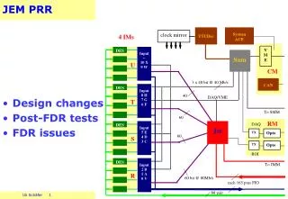
JEM 15 x 6-channel de-serialisers : SCAN921260 4 Input Processors : XC2V1500 Main Processor XC2V2000 6 links per de-serialiser DCS Input Processor Config VME VME Input Processor Main Processor Input Processor 6 ROC TTC G Input Processor G 15* '921260 88 LVDS links
PCB design issues • De-serialisers, TTCrx and XC2V are fBGAs with virtually no unused pins. 3 supply voltages (digital, analog, PLL) on de-serialisers. • High density of vias VCC/GND planes perforated need small vias, low clearances from via to GND/VCC high accuracy required • Huge PCB • PCB thickness increased to 2mm (compatibility) • Small via diameters not possible with thick PCBs • We need high VCC/GND distributed capacitance thin FR4 sheets/prepreg (shrinkage) reduced accuracy
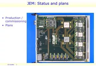
JEM1 Due to PCB issues, work on schematics has been discontinued and layout of a sub-set of the schematics was started: Preliminary layout of input block with 4 de-serialisers and one input FPGA is under way and is being discussed with the PCB manufacturer (Andus). • cost, technology (blind vias, micro vias,..?), timescale Fallback solution: old-style JEM 1.6mm, daughter boards ? Even though there won‘t be large amounts of (ATLAS) money spent on the first batch of JEM1s, a review will be appropriate due to technological challenges.
JEM1 First feedback from PCB manufacturer: • We share our problems with everyone using modern fBGA devices with full ball array as opposed to ring of balls. • Urged to go to 1.6mm PCB. It is no problem to have thicker board edges that fit the rails. Mechanical structures within a PCB are standard technology. Even integrated stiffeners are possible, if required. • With 1.6mm thickness 250 µm vias are possible. We are guaranteed to have 150µm of metal between two 1mm spaced vias. Recommendation for power planes: use GND/VCC/GND sandwiches throughout to increase distributed capacitance.
Full slice test Slice test will take place in x/2003 • JEM0.1 is available now • JEM0.2 is under production now • 1-2 JEM(s)0 will be submitted in (x-2.5)/2003 • Have JEMs1.0 available in ongoing slice test at a later stage • JEM1 seriously different from JEM0, expect minor PCB revisions (JEM1.1) for production modules