Download
1 / 15
150 likes | 285 Views
The Front-End Driver Card for CMS Silicon Microstrip Tracker Readout LEB2000 Krakow S.A.Baird, K.W.Bell, J.A.Coughlan, R.Halsall,W.J.Haynes, I.R.Tomalin CLRC Rutherford Appleton Laboratory E. Corrin Imperial College London Presented by John Coughlan. CMS Silicon Tracker Readout.

E N D
The Front-End Driver Card for CMS Silicon Microstrip Tracker ReadoutLEB2000 KrakowS.A.Baird, K.W.Bell, J.A.Coughlan, R.Halsall,W.J.Haynes, I.R.TomalinCLRC Rutherford Appleton LaboratoryE. CorrinImperial College LondonPresented by John Coughlan
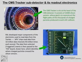
CMS Silicon Tracker Readout ~ 10 million Silicon Microstrips 80K APV25 readout chips ON Detector Analogue Optical readout 40K ADC readout system OFF Detector Level 1 rate ~ 100 kHz Front-End Driver: Optical receivers, ADCs, Digital processing, Buffering, DAQ interface Related talks... APV25 : Geoff Hall Optical Links : Francois Vasey LHC Test Beam : Nancy Marinelli Trigger Thottle System : Attila Racz Pixel Vertex Detector : Danek Kotlinski
FED Features • Functions • Optical Receiver • ADC • Digital Processing • Cluster Finding • Data Formatting • DAQ Buffering • Synchronisation Checking • Local Monitoring • Interfaces • Front-End Electronics • DAQ • TTC • Trigger Throttle & Synchronisation System • Detector Controls System
FED Architecture 1 OptoRx 1 1 Dual ADC Post ADC ASIC FE 1 PD Array Processing 6 Fibre ribbon 12 way Dual ADC 2 FPGA SSRAM 2 Prog Delay X DAQ READOUT fw SBC VME FPGA BSCAN 9 43 1 OptoRx 8 8 Dual ADC TTCrx Post ADC ASIC ASIC FE 8 PD Array Processing 48 Fibre ribbon 12 way Dual ADC DAQ FPGA Serial I/O RT Synch & Error Clock Prog Delay
Post ADC Processing Block trig hit trig1 trig2 trig3 token in cm sub Re-order 10 8 8 s-data 16 10 8 16 sync Hit finding ADC 1 8 data Ped sub d d Packetiser DPM 10 8 s-addr 8 8 Sequencer-mux a a No hits 8 averages headers hit trig1 trig2 trig3 cm sub Re-order 10 8 8 s-data 16 10 8 16 sync ADC 12 Hit finding 8 data Ped sub d d Packetiser DPM 10 8 s-addr token out 8 8 Sequencer-mux a a No hits 8 averages headers
FE FPGAs bus control etc SSRAM SBC VME FPGA VME Trigger in FPGA Ctrl Token out SSRAM INT Token back 8 1 FE FPGA 1 Prog Filter Format INT Data Merger Prog Filter Format 8 DAQ INT 8 DAQ X FE FPGA 8 TTC INT SSRAM INT 9 TTX Rx SSRAM Backend Readout Block
360 MByte/s FE 1 adc adc FE FPGA adc adc adc adc VME VME ’ 360 MByte/s FE 2 adc adc FE FPGA DSP adc adc ASIC adc adc 360 MByte/s adc adc adc 50 MByte/s/% FE 3 DAQ DAQ DSP FE FPGA adc adc ASIC adc adc 360 MByte/s fw adc FE 4 adc DSP FE FPGA NN Synch adc adc ASIC 100 KHz TTC adc adc TTCrx ASIC 360 MByte/s adc adc FE 5 DSP FE FPGA adc adc ASIC B Scan adc adc 360 MByte/s adc adc FE 6 DSP FE FPGA adc adc ASIC adc adc 360 MByte/s adc adc FE 7 FE FPGA DSP adc adc ASIC 150 MByte/s/% adc adc 360 MByte/s adc FE 8 FE FPGA DSP adc adc ASIC adc adc FED 9U Layout (96 ADC channels) • Board Input rate 3 Gbyte/s • Board Output Rate 50 Mbyte/s per percent occupancy
40 K ADC Channels 10 Bit@40MHz Trigger Rate 100 KHz Input Rate 1.5 T Byte/s Output rate 25 Gbyte/s/% Final System • 420 Boards 96 ADC/Board • 21 Crates • 7 Racks
Modelling as a tool Optimise the Design Optimising the cost performance ratio Elaborating & testing the Specification FED Modelling Basics Simulation Environment Digital HDL Simulator TTC - CLK... ‘VME’ Setup Param’s DAQ DAQ Output FED Model Test Bench ADC 0 Analyser Output Monte Carlo Test Vectors ADC N • Study • Buffer Depths & Overflow • Bus Speeds • Algorithm • Data Format • Exception conditions & handling • Data Flow control • Different operating scenarios….
Implementation 9U Design based on FED 1994 model Used in 1996 Beam Test 1 ADC Channel in ~25K Gate FPGA Limited at the time by FPGA technology FED Modelling Implementation No hits 8 fifo ctr Re-order trig1 trig2 trig3 trig2 token in write Baseline (average) Threshold (per strip) Pedestal Removal Quadrant data bus 10 8 sdata 10 8 8 sync adc 16 8 data Packetiser fifo 8 saddr token out 128 cycles 128 cycles proccessing status 8 fifo 8 Raw Data fifo • Additional Features • Re-ordering • Pedestal Removal • Threshold per strip • Data range monitoring & limiting • Sparsified & raw data readout
Software Architecture GUI Supervising WS Calibration Setup USER Tracker System ‘Kernel’ Network Network Network CRATE SBCs Real Time OS Fast Monitoring Exception Handling Tracker Crate ‘Kernel’ USER Hardware Driver VME Memory Map Hardware FED, FEC, TTC • Software Architecture • User Customisable within a RT framework Hit Finding Logic Analyser FPGA
FED Status & Plans • Interfaces Status • Opto Front-end specified (op-amp may be required) • TTC Rx concept well defined • Some areas less well defined, Throttle, Synchronisation (APV Emulation) • DAQ Specification not fully defined - DAQ TDR Q4/2001 • Modularity: FE-FED Mapping, Occupancy, DAQ Rates, load balancing • Timescales • PMC Prototype satisfies Labs and Test Beams 1999-2001 • Design & Modelling of Final FED until mid 2001 • (Clustering algorithm ) • Final FED Prototype for test beam 2002 • Final FED Production start in 2003
8 x 10 Bit 40 MHz ADC 64K Memory/per ADC 40 K Gate FPGA Control PCI Interface Mounts on Commercial VME CPU Board (or with an adapter in a PC slot) FED-PMC Prototype • 30 in service • 30 more about to be ordered • Present Generation of ADC PMC • Used in LHC test beam Y2000
Tracker Monitoring & Control 50K ADC Channels 1 25 VME SBC RTOS FED CRATES E-Net Switch • Trigger Rate 100 KHz • Input Rate from FE 1.5 T Byte/s • Output rate to DAQ 25 Gbyte/s per percent occupany Tracker Control WS FEC CRATES TTC CRATES D-BASE DAQ R/C DCS
Crate Layout 1 2 21 FE 1 LAN FE 2 100MBit/s FE 3 FE 4 DAQ FE 5 TTC 100 KHz FE 6 Throttle FE 7 NN Synch F-Bus FE 8 B-Scan • Crate Input Data Rate 60 Gbyte/s • Crate Output Data Rate 1GByte/s per pecent occupancy