Download
1 / 18
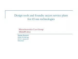
180 likes | 489 Views
65 nm activities. Marseille group ATLAS-CMS 65 nm pixel ASIC workshop 26 November 2012. Outline. Introduction Prototype chip for ATLAS pixel SEU test results Total dose effects Perspectives for this work Other proposed IP blocks designed under the AIDA WP3.3 Conclusion.

E N D
65 nm activities Marseille group ATLAS-CMS 65 nm pixel ASIC workshop 26 November 2012
Outline • Introduction • Prototype chip for ATLAS pixel • SEU test results • Total dose effects • Perspectives for this work • Other proposed IP blocks designed under the AIDA WP3.3 • Conclusion ATLAS-CMS 65 nm pixel ASIC workshop
Motivations • For the HL-LHC (Phase 2) a new pixel detector is planned • 2 removable internal layers are planned ( 3.9 cm – 7.5 cm) • The event rate is high and the FE-I4 architecture is not adapted • A new design is required • Reduction of the pixel size for the inner layers • R&D : CMOS 65 nm, 3D, Monolithic design • CMOS 65 nm is an attractive solution for the development of high-density readout IC 400 μm 50 μm FE-I3 CMOS250 nm 250 μm FE-I4 CMOS 130 nm 50 μm 150 μm 25 μm FE-I5 CMOS65 nm ATLAS-CMS 65 nm pixel ASIC workshop
ATPIX65A: Atlas Pixel prototype array • ATPIX65 : small array of pixels 16x32 designed at Berkeley using 65 nm CMOS process • Pixel area : 25 µm x 125 µm • Pixel Configuration : 8 Triple Redundant Latch (TRL) with error correction • Data loaded and read back with shift register (SR) . • 16 columns of 256 Configuration TRL and 256 DFF • Design based on standard cells from ARM library 16 X 32 array 25m X 125m pixels Pixel Configuration block Datain Majority logic Latch1 sel Latch2 Latch3 ATLAS-CMS 65 nm pixel ASIC workshop
SEU test results • IRRAD3 beam line of the CERN Proton Synchrotron (PS) • Beam of 24 GeV protons with a spot area around 1 cm² • Reach a fluency of 1 - 3 1013 p/cm2 per hour • Data acquisition based on FPGA and synchronized with the spill signal • SEU rate is computed for the TRL (configuration cell) and for the DFF (shift register unit cell) • TRL cell is170 times more tolerant than a DFF • Improvement by factor 4 compared to the FE-I4 configuration cell • MBU (Multiple Bit Upsets) were observed for the DFF but the ratio still low • Successive DFF separated by 4-6 µm TRL = 2.6 10-16 cm² DFF = 4.5 10-14cm² DFF / TRL = 170 ATLAS-CMS 65 nm pixel ASIC workshop
Dose effects • At high levels of dose systematic errors appear in the configuration memory • The state of some DFF cells remains stuck to 0 or 1 • 2 chip were irradiated with 24 GeV proton beam • Chip 1 : irradiated up to 870 MRad: 3 spill/cyle without annealing • Systematic errors start to appear from 350 Mrad • Chip out of the beam : we still have errors but the number of errors decreases with annealing effect • Still have errors after 420 hours of annealing • The chip 1 had a floating analog bias • Chip 2 irradiated up to 435 MRad: 1 spill/cycle and annealing during 10-20 hours each 10-20 MRad • Systematic errors start to appear from 350 Mrad 870 MRad 770 MRad 640 MRad 350 MRad 470 MRad 320 MRad ATLAS-CMS 65 nm pixel ASIC workshop
Dose effects on the 65 nm device • The leakage current increases by 1 order of magnitude for a total dose of 435 MRad • No threshold voltage shift up to 100 MRad but more pronounced from 200 MRad • Narrower devices (W=150nm-200nm for digital) should show more shift on the threshold • More irradiation tests have to be done (Xray irradiation at CERN?) • For Chartered 130 nm process Xray irradiation did not show such a high dose behavior observed with proton • Special layout rules have to be defined for digital cells when the TID have to exceed 200 MRad ATLAS-CMS 65 nm pixel ASIC workshop
Perspectives • Good results in term of cross section and tolerance to SEU • Dose effect is under study and more irradiation tests have to be done • Digital library have to be developed • A new design is now under development • Design tolerant to a total dose of 500 MRad • Improve the SEU tolerance of the unit cell to be implemented in the global memory • Memory for global configuration • An array of 1 kbit ? • Triplicate the Majority Logic • Minimize the effect of glitches • First submission in 65nm CMOS foreseen in 2013 • Other 65 nm IP blocks Datain Majority Logic Latch1 sel Latch2 t Latch3 2t ATLAS-CMS 65 nm pixel ASIC workshop
Generic ADC for monitoring • General purpose ADC • Inputs are slow variation signals : • Temperature, leakage current … • Clock frequency : 100 kHz -1 MHz • Architecture : Successive Approximation Register (SAR) • Precision : 10 bit (12bit ? If required) • DC accuracy : • Integral linearity error : +/- 1 bit • Differential linearity error +/- 0.5 bit • Voltage Reference provided by an external IP block • Operating input voltage : 0-Vref • Conversion time : 12-14 clock cycles • Tolerance to a TID of 500 MRad out 10 bit SAR ADC Analog MUX inputs Vin status clk start enable select ATLAS-CMS 65 nm pixel ASIC workshop
Bandgap reference • Bandgap Reference for general purpose provide voltage reference for : • Biasing, DAC, ADC … • 2 Voltages : to be defined (0.8 V? and 0.6 V?) • Temperature : from -50 °C to 120 °C • Temperature coefficient : 400 ppm/°C max • Voltage coefficient : TBD • Start up circuit • CLoad MAX = 20pF and RLoad = 10 MOhm • Power supply = 1.2 V • Power consumption • Noise < 20 µV RMS • Radiation hard : 500 MRad Vdda Bg_outa en BGVR Bg_outb Gnda ATLAS-CMS 65 nm pixel ASIC workshop
Temperature Sensor • Precision : +/- 1 °C • Functional temperature range -40 to +60 °C • Sensitivity better than 0.6 mV/°C • Radiation tolerance : 500 MRad • Correction of the irradiation effect Vbn Vdda out en TempSens Gnda ATLAS-CMS 65 nm pixel ASIC workshop
Conclusion • TSMC 65 nm process allows good tolerance to SEU • The tolerance of TSMC-ARM digital cells have to be investigated for a high dose levels : 350-500 MRad • Simulations are in progress to check if there are “sensitive” devices inside the Library DFF cell • A new design with different structures of configuration memories in under development • IP blocs : ADC, Voltage reference, Temperature Sensor are under design • First submission of 65nm CMOS IP blocks is foreseen in 2013 ATLAS-CMS 65 nm pixel ASIC workshop
Back up slides ATLAS-CMS 65 nm pixel ASIC workshop
Dose rate during the test ATLAS-CMS 65 nm pixel ASIC workshop
Dose effects on the 65 nm device • Measurement of proton radiation effects on a 65nm transistors • nMos low Vt transistor with W/L=22µm/100nm • This measurement have to be done on a minimum area device • Understand the effect for the dose level higher than 200 MRad • The leakage current increases by 1 order of magnitude for a total dose of 200 MRad • The leakage current seems to reach a saturation value for high dose levels but grows up from a dose level of 200-300 MRad • Is the dose effect on the configuration memories related to a minimal size transistor used in digital cells from ARM library ? ATLAS-CMS 65 nm pixel ASIC workshop
SEU test results Errors plot for the Shift register DFF Errors plot for the configuration cell (TRL) • SEU rate is computed for the DFF cell and for the TRL • Cross section : • TRL = 2.6 E-16 cm² • DFF = 4.5 E-14 cm² All patterns All patterns Pattern 0000 Pattern 0000 Pattern 1111 Pattern 1111 Rows 0-255 Rows 0-255 Columns 0-15 Columns 0-15 Columns 0-15 Columns 0-15 Columns 0-15 Columns 0-15 TWEPP 2012, Oxford University, UK
Dose effects 260 MRad to 310 MRad 390 MRad to 420 MRad • From a dose level of 260 MRad : • Systematic errors begin to appear for patterns “0000” or “1111” • The effect increases with the dose and cover the half of the DFF cells at 640 MRad • The effect persists even outside the beam • After Annealing, the number of systematic errors decreases • The chip seems to go back to a normal behavior after 420 hours of annealing • But, still have a lot of errors with the pattern “1010” • A new chip is currently being tested to check if the results are repetitive Pattern 1111 Pattern 1111 Rows 0-255 Rows 0-255 Columns 0-15 Columns 0-15 Number of errors for column 5 TWEPP 2012, Oxford University, UK
Error rate estimation for pixel configuration • The SEE fluency is calculated by summing the rates of charged particles (hadrons) and neutrons with kinetic energies > 20MeV. • the estimated SEE rate based on simulations for the LHC, is 0.23 E15 hadrons/cm²/year for the pixel B-layer • For the HL-LHC (phase2), the luminosity is 10 times higher than at the start of the LHC. If we consider 1 year =1E7 sec, we have 2.3 E8 part/cm2.s • The rate for 1 latch = 4.6 E-8 SEU/s -> 0.0645 SEU/s for a 65nm chip


![Nm]](https://cdn3.slideserve.com/6300766/slide1-dt.jpg)