Download
1 / 14
140 likes | 369 Views
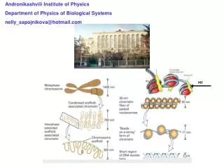
E. L. Andronikashvili Institute of Physics Georgian Academy of Sciences. Presented by Prof. Nugzar Zoidze Lisbon, 2-4 December, 2002. History of institute.

E N D
E. L. Andronikashvili Institute of PhysicsGeorgian Academy of Sciences Presented by Prof. Nugzar Zoidze Lisbon, 2-4 December, 2002
History of institute • Initially the Institute of Physics in Georgia was founded in 1935 at the Tbilisi State University. Since 1950 it belongs to the Georgian Academy of Sciences. • At the Institute of Physics the research is carried out in the following fields: • Particle Physics • Physics of Condensed Matter • Plasma Physics • Physics of Biological Systems • Thin Film and Nano Technologies
Current Activities of the Institute • Particle PhysicsThe main activity in Particle Physics is concentrated around the projects realized at the large elementary-particle accelerators • Condensed Matter PhysicsIn the field of Condensed Matter Physics the current activities are concentrated around the problems of • Real Crystals • Interaction of dislocations with point defects • Anisotropic growth, swelling and creep processes • Distribution of the electric charge near the dislocations in the ionic crystals) • Magnetic Phenomena in Solids • Dynamic and dissipative processes in non-linear regimes of the spin-systems at low and ultralow temperatures
Current Activities of the Institute • Plasma Physics In the field of Plasma Physics the development of the Theory of Non-linear Phenomena is one of the main directions. Among other problems the peculiarities of kinetic processes in Tokamaks were established. • Physics of Biological SystemsThe main activities in Physics of Biological Systems are connected with the study of Thermodynamics of proteins, nucleic acids and their complexes, content and role of metals in nucleic acids. • Thin Film and Nano TechnologiesIn the field of Thin Film and Nano Technologies development there was established mechanism of electroless deposition of various metals and alloys, developed new competitive technologies of melallization at surface treatment.
Method of Metallization of Powder-Like Particles, Diamond and Bulk Carbon • Methods allow to obtain nanostructured composite materials and coatings: • with the specified catalytic activity, • metal-coated fullerenes, • metallized carbon nanotubes, • conductive nano-sized additives to plastics and rubber, • nanoparticle-reinforced tires, • novel sensors, • detectors of chemical and biological agents, • unique catalysts, • adsorbents, • hydrogen storage materials, etc.
Investigation of the mechanism of activation for electroless plating • O O- O O- O O- \\ / \\ / \\ / P +OH-H+cat P +H-ad+ H+cat P + H + e + H+[1] / \ / \ / \ H H H O-H H O-H • H2PO2- + e P + 2 OH-[2] • Ni (II) +2e Ni [3] • H+e+H+ H2[4] • Ni2+ + 2H2PO2- + 2H2O Ni + 2H2PO3- + H2 + 2H+[5] • Sn (II) + Pd (II) = Sn (IV) + Pd [6] • PdCl42- + H2PO2- + H2O Pd + H2PO3- + 2H ++ 4Cl -.[7] • 2 HCl + PdCl2 = H2PdCl4, [8]
Cr (VI)-Free Electroless and Electrochemical Hard Coatings of Ni-W and Ni-B-W Alloys • The method of obtaining hexavalent chromium-free electroless and electrochemical hard coatings deposited from non-toxic solutions on mild steel, stainless steel, etc. was developed. Importance of the simultaneous increase in wear and corrosion resistance by the proposed method is emphasized by the fact that the cost of corrosion has been estimated in excess of $ 200 billion and the cost of wear – at about $ 50 billion per year for the USA economy.
Main advantages • There is no very toxic hexavalent chromium, chromic acid or cyanide • The microhardness and wear resistance of proposed coatings exceeds that of the corresponding chromium coating • The proposed coatingsare high temperature- and corrosion-resistant • The current efficiency of the proposed method is 7 times higher as compared to chromium electrodeposition • Coating uniformity and throwing power are significantly higher as compared to electroplating of chromium
A New Device for Determination of Ductility by Bending • A significant advantage of the suggested device is its capability to measure the ductility at different rates of deformation and at low temperatures. • The importance of this advantage is proved by the following data given in literature: • the 10-fold increase (in some cases) in the strain value at the 10-fold increase in the deformation rate; • the increase in the internal stress proportional to the deformation speed; • the jump-like increase in the strain value with the increase in the deformation rate at transition from the superconductive state to the normal state.
Fig. New device for determination of ductility by bending(constructed by T. Khoperia) 1 – wedge-shaped support; 2 – pressure shafts; 3 – arrows showing the specimen bending; 4 – scale calibrated in degrees; 5 – flywheel, by rotating of which lowering of the pressure shafts and bending of the specimen are provided from the opposite sides of the wedge- shaped support; 6 – microscope; 7 – specimen under testing; 8 – spring; 9 – rod for pressure shafts; 10 – support of a spherical shape; 11 – electromotor; 12 – gear box; 13 – gear
Application of Technologies • The developed technologies could be be used in the following fields of industries: • Electronics & Microelectronics • Photonocs & Instrument making • Machine building & Powder metallurgy • For production of cutting and drilling instruments • Batteries & Fuel cells • For solar energy conversion into electrical energy and splitting of water using solar energy • Medicine practice & Ecology • For production of catalysts & in chemical industry • Air space techniques
List of Cooperation Partners in CIS and Abroad • University of Tokyo Fujishima Laboratory Department of Applied Chemistry School of Engineering • Broddarp of Nevada, Inc. USA • Fraunhofer Institute for Reliability and Microintegration (IZM), Dept. of Mechanical Reliability and Micro-Materials, Germany, • EADS, Germany • Institute of Physical Chemistry, Russia.
Type of Cooperation We are Looking for • Joint investigations • Testing of the samples fabricated by our methods • Joint patenting • Implementation of technologies at foreign enterprises and companies • Sale of technologies • Establishment of joint ventures, etc.
Contact information Address: Institute of Physics. 6, Tamarashvili str., Tbilisi, 380077, Georgia http://www.iph.hepi.edu.ge E-mail: postmaster@iph.hepi.edu.ge FAX: (+995 32) 536937