Download
1 / 33
370 likes | 590 Views
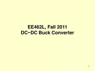
Design of a Digital Controller Chip for a DC-DC Buck Converter. Dr. Amit Patra Ravinder Pal Singh Bhaskar Goswami. Motivation. DCDC, DCDC-B, DCDC-BT tested. Why Digital controller ? Inherently lower sensitivity to process and parameter variation Programmability

E N D
Design of a Digital Controller Chip for a DC-DC Buck Converter Dr. Amit Patra Ravinder Pal Singh Bhaskar Goswami
Motivation • DCDC, DCDC-B, DCDC-BT tested. • Why Digital controller ? • Inherently lower sensitivity to process and parameter variation • Programmability • Noise immunity, small size and lower power
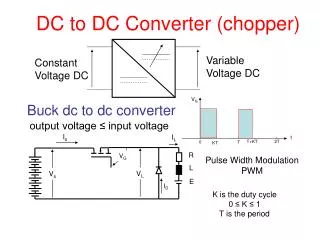
Vo- E= -L di di dVo dVo dt dt =C =C dt dt IP L Ton = E -Vo Vo= - L IP L Toff = Vo Vo Vo ( i - ) ( i - ) R R D C Load V Gate Pulses During charging: t Ton Toff iL Inductor Current IP During discharging: t IP L is constant. => constant Volt-sec. Hence the name Bang-Bang Control.
Scheme Vout E D C Load C(t) Vout Buffer Controller (Variable Frequency Variable Duty Cycle) EN E Buffer Comparator Vref K Vref Buffer Digital Controller IC
Specifications • Input 2.5V-3.75V • Output 1.2V-1.8V • ADC 6 bit resolution • IP 500mA • L 100uH • Clock 2.5MHz • Process CMOS8 • Approx. Area 3mm X 3mm
What do we get out of it? • No Reverse Recovery Losses in the Diode • Circuit Implementation is Simple • Use of ADC & Voltage Reference make the output voltage free of load or supply line effect • Soft Start Feature
Delay line A/D converter VDD Vin Vout
VDD (Vin) TEST RESET VDD (Vin) TEST Delay1 Delay2 Delay1 Delay Delay DelayN RESET FF FF FF SAMPLE A[0] A[1] A[2] Delay Block
VDD High (Less Delay) 1 1 Td 1 1 0 SAMPLE
VDD Low (More Delay) 1 1 0 0 0 SAMPLE
Encoder and Calibration • Encoder converts Thermometer Code to Binary Code • Any Error due to ADC is calibrated by a Calibrator
Integral Non Linearity Max INL – 0.22
Differential Non Linearity Max DNL – 0.22
ADVANTAGES & DISADVANTAGES • Advantages • Doesn’t require high precision analog components. • Require less power, less chip area. • Doesn’t require S/H circuit or low pass filter. • Less sensitive to noise, specially suitable for switching power converters. • Disadvantages • INL & DNL are poor.
Gate Pulse Controller TON = K/(Eactual – VOUT) TOFF = K/Vout
Process & Tools Used • Designed by 0.25 micron Technology & been sent for fabrication to NSC in April • Digital parts described by Verilog HDL • Synopsys tools used for Synthesis & Timing • Cadence tools are used for simulations • Chip layout – Avanti’s place & route tool, LVS, DRC • Chip Package - PLCC
Testing Scheme • K = Ip×L can be provided externally • Reference Voltage can be fed from outside • Outputs of the ADC taken out • In case ADC fails, Digital Vout, Vref, E can be provided externally • The mode of operation, described by Enable, taken out to study the operations of Comparator, etc.
Scope of Future Work • PMOS Switch • Scheme for the improvement of INL of the ADC • Use of over sampling ADC • Controller at Sleep Mode • Different Control Action possible by using RAM inside the Controller
References • R. W. Ericson, D. Maksimovic, Fundamentals of Power Electronics, 2nd edition, Kluwer Academic Publishers: 2000. • G. F. Franklin and J. D. Powell, Digital Control of Dynamic Systems, Addision – Wesley Publishing Company, Inc.: 1998. • A. Prodic, D. Maksimovic, R. Erickson, “Design and implementation of a digital PWM controller for a high-frequency switching DC-DC power converter,” IEEE IECON 2001 • J. Xiao, A. V. Peterchev, S. R. Sanders, “Architecture and IC implementation of a digital VRM controller,” IEEE PESC 2001, pp. 38-47. • B. J. Patella, A. Prodic, A. Zirger, D. Maksimovic, “High-frequency digital controller IC for DC/DC converters,” Applied Power Electronics Conference and Exposition, 2002. APEC 2002. Seventeenth Annual IEEE, Volume: 1, 2002, pp. 374-380. • Phillip E. Allen, Douglas R. Holberg, CMOS Analog Circuit Design, 2nd Edition, Oxford University Press, 2002 • Samir Palnitkar, Verilog HDL – A Guide to Digital Design and Synthesis, Pearson Education Asia