Download
1 / 1
10 likes | 145 Views
Hybrid Behavioral-Analytical Loss Model for a High Frequency and Low Load dc-dc Buck Converter. D. Díaz.

E N D
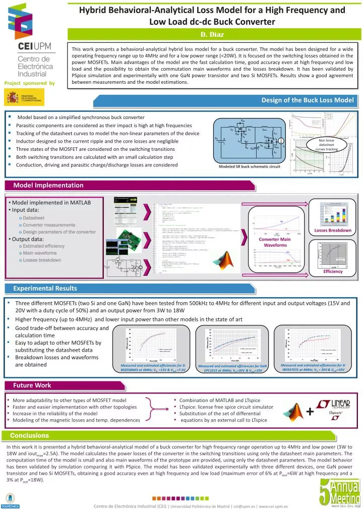
Hybrid Behavioral-Analytical Loss Model for a High Frequency and Low Load dc-dc Buck Converter D. Díaz This work presents a behavioral-analytical hybrid loss model for a buck converter. The model has been designed for a wide operating frequency range up to 4MHz and for a low power range (<20W). It is focused on the switching losses obtained in the power MOSFETs. Main advantages of the model are the fast calculation time, good accuracy even at high frequency and low load and the possibility to obtain the commutation main waveforms and the losses breakdown. It has been validated by PSpice simulation and experimentally with one GaN power transistor and two Si MOSFETs. Results show a good agreement between measurements and the model estimations. Project sponsored by • Design of the Buck Loss Model • Model based on a simplified synchronous buck converter • Parasitic components are considered as their impact is high at high frequencies • Tracking of the datasheet curves to model the non-linear parameters of the device • Inductor designed so the current ripple and the core losses are negligible • Three states of the MOSFET are considered on the switching transitions • Both switching transitions are calculated with an small calculation step • Conduction, driving and parasitic charge/discharge losses are considered Non linear datasheet curves tracking Modeled SR buck schematic circuit Model Implementation • Model implemented in MATLAB • Input data: • Output data: • Datasheet • Converter measurements • Design parameters of the converter Losses Breakdown Converter Main Waveforms • Estimated efficiency • Main waveforms • Losses breakdown Efficiency Experimental Results • Three different MOSFETs (two Si and one GaN) have been tested from 500kHz to 4MHz for different input and output voltages (15V and 20V with a duty cycle of 50%) and an output power from 3W to 18W • Higher frequency (up to 4MHz) and lower input power than other models in the state of art • Good trade-off between accuracy andcalculation time • Easy to adapt to other MOSFETs bysubstituting the datasheet data • Breakdown losses and waveformsare obtained Measured and estimated efficiencies for Si IRFR3707Z at 4MHz; Vin = 20V& Vout=10V Measured and estimated efficiencies for Si BSZ058N03 at 4MHz; Vin =15V & Vout=7.5V Measured and estimated efficiencies for GaN EPC1015 at 4MHz; Vin=20V& Vout=10V Future Work • More adaptability to other types of MOSFET model • Faster and easier implementation with other topologies • Increase in the reliability of the model • Modeling of the magnetic losses and temp. dependences • Combination of MATLAB and LTspice • LTspice: license free spice circuit simulator • Substitution of the set of differential • equations by an external call to LTspice + Conclusions In this work it is presented a hybrid behavioral-analytical model of a buck converter for high frequency range operation up to 4MHz and low power (3W to 18W and ioutmax=2.5A). The model calculates the power losses of the converter in the switching transitions using only the datasheet main parameters. The computation time of the model is small and also main waveforms of the prototype are provided, using only the datasheet parameters. The model behavior has been validated by simulation comparing it with PSpice. The model has been validated experimentally with three different devices, one GaN power transistor and two Si MOSFETs, obtaining a good accuracy even at high frequency and low load (maximum error of 6% at Pout=6W at high frequency and a 3% at Pout=18W).