Download
1 / 29
550 likes | 1.63k Views
Thermal diffusion, Ion implantation. sami.franssila@aalto.fi. Doping: modifying resistivity. Gas phase diffusion Solid source diffusion Ion implantation e.g. POCl 3 gas e.g. boron-doped film 20-200 keV ions at 1000 o C at 1000 o C at room temperature

E N D
Thermal diffusion,Ion implantation sami.franssila@aalto.fi Microfabrication
Doping: modifying resistivity Gas phase diffusion Solid source diffusion Ion implantation e.g. POCl3 gas e.g. boron-doped film 20-200 keV ions at 1000oC at 1000oC at room temperature Oxide mask Oxide mask Resist mask
Doping vs. resistivity Single crystal silicon resisitivity is lower than that of polysilicon, for same doping concentration.
Two modes of diffusion Fixed supply of dopant: when dopant atoms diffuse into silicon, surface concentration decreases Infinite supply of dopant: New supply of dopant keeps surface concentration constant when dopant atoms diffuse into silicon Microfabrication
Fixed source vs. infinite source Longest diffusion time Longest diffusion time Fixed number of dopantatoms “Infinite” initial dopant atoms
MOS-controlled thyristor Multiple diffusions: -deep p diffusion -heavy n+ diffusion -intermediate n diffusion -shallow p+ diffusion -heavy p+ diffusion on back Microfabrication
Multiple diffusion (2) Take n-silicon wafer Perform p-diffusion p diffusion N-silicon 3. Perform n-diffusion p-diffusion becomes deeper N-concentration must be higher than p; otherwise dopant type does not change. N-diff p diffusion N-silicon Microfabrication
Diffusion profiles When n-dopant concentration is high enough, p-type silicon turns n-type. This n-type silicon can be turned to p-type again, by applying even enough boron concentration.
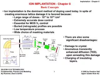
Ion implantation(Chapter 15) • Ion-solid interactions • Dopant profiles • Implant damage and damage anneal • Implant equipment • Implant applications Microfabrication
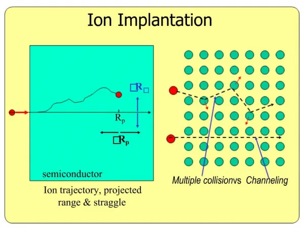
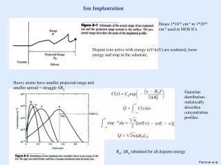
concentration ΔR Rp depth Basic implantation process Accelerated ions (B+, P+, As+) hit silicon, penetrate, collide randomly and come to rest. Photoresist mask. Peak concentration is inside silicon resist <Si> Microfabrication
Implant parameters Ion energies 10-200 keV Implant depths 10-500 nm Doses 1011 to 1016 ions/cm-2. Concentrations ca. 1015 cm-3 to 1020 cm-3. 5.1015 cm-2 ion implant dose and depth of ca. 200 nm translates to ca. 25 Ohm/sq sheet resistance Microfabrication
Projected range and straggle Ion (P), dose (1014 cm-2), energy (100 keV) Straggle Projected range Microfabrication
Projected Range (Rp) in Si Rp (μm) Rp depends on incident and target atomic masses • In practise, • 200 keV max • Boron 500 nm • Phophorous 200 nm • Arsenic 100 nm Ion energy (keV) Microfabrication
Implant profiles 100 keV; B, P, As into silicon Implantation thru 200 nm thick oxide (50 keV vs. 150 keV) Microfabrication
Implant profiles (2) As a function of energy: P+: 50, 100, 150 keV energies As a function of dose P+ doses: Microfabrication
Stopping process: stochastic collisions Microfabrication
Implantation damage Light ions like boron, and low doses (<1014 cm-2) cause mainly point defects High doses (>1015 cm-2) and heavy ions (As+, Sb+, Ge+) cause extended damage and amorphization Microfabrication
implant damage electrical activity dopant solubility dopant diffusivity Implant dose, damage and anneal Damage has to be annealed away. Temperatures are ca. 1000oC ( implantation is a high temperature process !) Crystalline defects annealed. Dopants find their place in the crystal lattice. Microfabrication
Annealing after implantation • implantation is a room temperature process • silicon crystal is damaged by high energy ions • this damage is annealed away at ca. 1000oC • implantation always requires high temperature just like thermal diffusion (but easier process sequence by elimination of oxide)
wafer chamber Faraday cup load lock selection magnet acceleration tube ion optics extraction ion source gas 1 gas 2 Main elements of an implanter Microfabrication
Implanter equipment • Generation of ions – dopant gas containing desired species • BF3, B2H6, PH3, AsH3, AsF5 • – plasma provides positive ions • 11B+, BF2+, 31P+, 31P++ • Ion extraction • ions are extracted from the source due to a high electric field • Ion selection • magnetic field mass analyzer selects the appropriate ion (mass & charge) • Ion acceleration • further accelerate ions giving the ions their final kinetic energy. • Beam scan / Disk scan • provides a uniform dose of ions over the wafer surface. • In-situ dose monitoring Microfabrication
Diffusion vs. implantation Doping by diffusion: Oxide mask for diffusion MOS gate needs to be aligned to S/D junctions misalignment Self-aligned gate by implantation: polysilicon gate blocks ions, and MOS channel remains undoped Microfabrication
Implantation vs. diffusion • Implantation is more accurate in dose control • Implantation produces greater variety of profiles • Implantation is possible through the surface layers • Sideways spreading is 1/3 of the vertical range in implantation and isotropic in duffusion • Diffusion is high-temperature process, implantation is room temperature process • Damages after implantation are annealed at high temperature • Diffusion is the best for high doping level, deep junctions and double side doping Microfabrication
Doping of epi films Gas phase dopant molecules are mixed in silane flow: 2 PH3 2 P + 3 H2 B2H6 2 B + 3 H2 Epitaxial films come in all the same varieties as silicon wafers: -n-doped -p-doped -high resisitivity (not intentionally doped) Benefits of epi: Oxygen and carbon of the substrate wafer are buried under epi. Dopantuniformity is very good.
Epi doping Add gaseous dopants into the flow: B2H6 for boron PH3 for phoshorous AsH3 for arsenic Very small partial pressures enough: 10-10 bar 1015 cm-3 10-8 bar 1017cm-3 10-6 bar 1019cm-3
Epitaxy temperatures Reactor cleaning before each wafer. In-situ wafer cleaning to ensure the best possible cleanliness.
Dopant diffusion during epi Because epitaxy is a high temperature process, dopant atoms diffuse during epitaxy. Diffusion is from high dopant concentration to low concentration. Epi doping level is independent of substrate doping level, but the interface is not sharp due to diffusion. Lightly doped epi Heavily doped substrate