Download
1 / 15
330 likes | 834 Views
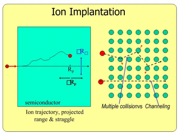
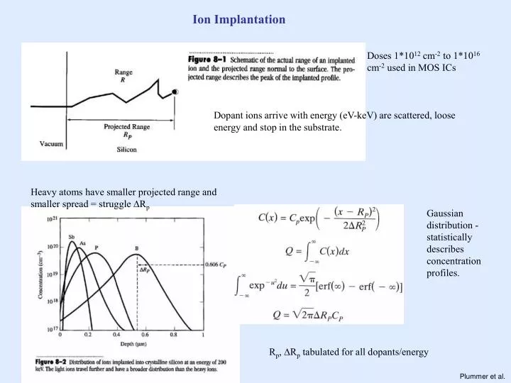
Ion Implantation. Doses 1*10 12 cm -2 to 1*10 16 cm -2 used in MOS ICs. Dopant ions arrive with energy (eV-keV) are scattered, loose energy and stop in the substrate. Heavy atoms have smaller projected range and smaller spread = struggle R p.

E N D
Ion Implantation Doses 1*1012 cm-2 to 1*1016 cm-2 used in MOS ICs Dopant ions arrive with energy (eV-keV) are scattered, loose energy and stop in the substrate. Heavy atoms have smaller projected range and smaller spread = struggle Rp Gaussian distribution -statistically describes concentration profiles. Rp, Rp tabulated for all dopants/energy Plummer et al.
Energy Dependence Rp and Rp for dopants in Si. Plummer et al.
3D Distribution of P Implanted to Si Rp =50 mm, Rp =20 mm Lateral struggle R Plummer et al.
Masking Layer in Ion Implantation Photoresist, oxide mask Lateral struggle important in small devices Dose that penetrates the mask Masking should be efficient including the annealing steps The criterion for efficient masking To stop ions: Under the poly-Si gate Plummer et al.
Implantation Followed by Annealing Function rediffused Annealing requires additional Dt terms added to C(x) Cp, depth , C(x) remains Gaussian. Backscattering of light atoms. C(x) IS Gaussian only near the peak. Plummer et al.
Implants in real Silicon – The role of the Crystal Structure (Symmetry) Orientation effects are important both for Si and MEMS processing (110) C –Si appears random at the surface channeling possible (100) Plummer et al.
Channeling Effect As two profiles Dual-Pearson model gives the main profile and the channeled part. Dependence on dose: damage by higher doses decreases channeling. No channeling for As @ high doses! Parameters are tabulated (for simulators) Include scattering in multiple layers(also masks’ edges). This is important for small structures/devices Screen oxide decreases channeling
Manufacturing Methods and Equipment Mass Analysis Centrifugal force Lorentz force Ion velocity B++, B+, F+, BF, BF2+ Ion beam deflected to remove neutrals Mass Selection mr Gives mass separation AsH3 PH3 BF2 in 15% H2 Very toxic Integrate the current to determine the dose Ion beam heating due to bombardment. In-situ annealing leads to defects
High Energy Implants Applications in fabrication of: wells (multiple implants give correct profiles ex. uniform or retrograde), buried oxides, buried layers (MeV, large doses)! - replace highly doped substrate with epi-layers Twin well design CMOS In latch-up Thyristor structure. Here the p-well is of the same conductivity type as the substrate. UEB 0.7V P-well p-n-p n-p-n UBE 0.7V See devices in notes #3.1 Decrease of Rsub - less latch-up Future IC fabrication: implantation at high energy becomes more important - reduction of processing steps
Models and Simulations • Rutherford(1911) - (He) backscattered due to collision with a + nucleus. • Bohr- the nuclear energy loss due to + atoms cores and electronic loss due to free electrons decrease many contributors. • Lindhard, Scharff and Schiott (1963) (LSS) Nuclear Stopping Z2, m2 Elastic collisions Computers used to find the range R Scattering potential Role of electrons Thomas-Fermi model Energy transferred Head-on collision (max. Energy transfer) Nuclear stopping power
Electronic Stopping Nonlocal A polarization of the dielectric minimizes the E field drag force ion velocity and depends on effective ionization. ion As in particle transport in a viscous medium Energy loss w/o the trajectory change Inelastic Collisions with electrons momentum transfer, small change of the trajectory. Local Energy loss depends on ion, substrate&particular topping mechanism Close: wave functions overlap Total Stopping Powers Electronic and Nuclear mechanisms are important. Channeling should be also included MC simulation
Damage Production Displacement energy (for a Frenkel pair) 15eV large damage induced by Ion Implantation 30 keV As Rp 25mm E decreases to Ed so that ions stop. Si Si Si Si Dose – large damage
Damage Annealing Formation of End-of-Range (EOR) defects @ a/c interface in Si large damage after II @ the C-Si side but below the threshold for amorphization. Loops R= 10 nm grow to 20 nm in 1000 °C Furnace 850 °C RTP 1000 °C Solid Phase Epitaxy 5 min 1 sec 60 min 60 sec 400 sec 1000 °C gives stable dislocation loops 960 min 1100 °C/60 sec may be enough to remove the dislocation loops . Loops in P-N junctions leakage Optimize annealing: Short time, high T to limit dopant diffusion but remove defects Optimize I2 : LN2 Ge 4*1014 cm-2 RT- 5*1014 cm-2 @ RT , EOR @ 100 nm depth =25 nm, 1010 cm-2 @ 900 °C/15 min @ LN2 NO EOR!
Solid State Epitaxy Regrowth from the C-Si acting as a seed (as in crystal growth from melt) Fast regrowth @ 600 deg C, 50 nm/min <100> 20 nm/min <110> 2 nm/min <111> 2.3 eV is for Si-Si bond breaking Regrowth rate Dopants are active =substitutional position with very little diffusion. But high T might be needed for EOR annealing. No defects= no diffusin enhancement Time increases
Dopant Activation – No Premorphization Low T Annealing is enough for low doses – low primary damage can be easily annealed. High doses – damage below amorphization secondary defects = difficult to anneal and requires high T 950-1050 ° C. High initial activation, full activation is fast @ low T, Low initial activation, traps anneal out, I compete with B for substitutional sites, I –B complexes More damage so activation decreases with dose maintaining the same behavior. (1) (2) (3)