Download

1 / 51
510 likes | 758 Views
ADC Student Lecture. Andrew Brown Jonathan Warner Laura Strickland. Table of Contents. Signals Applications of ADC’s Types of ADC’s Successive Approximation Example The ADC on the MC9S12C32. Introduction.

E N D
ADC Student Lecture Andrew Brown Jonathan Warner Laura Strickland
Table of Contents • Signals • Applications of ADC’s • Types of ADC’s • Successive Approximation Example • The ADC on the MC9S12C32
Introduction • Analog to digital converters convert analog, or “real world” signals to a series of 1’s and 0’s, able to be stored or transmitted through computers or digital systems.
Introduction cont. • Reasons why this would be needed: • Digital storage of a non-digital signal • (ex: recording light intensity of a lightning strike using sensors, mapping a flight path of an aircraft onto a computer for analysis) • Transmitting data over a digital system • (ex: sending your voice through a telephone system,Skype chatting, etc…)
Analog Signals • Analog signals are the smooth, “real”, signals of the world. • These signals can contain any and all values needed to represent the data in question.
Digital Signals • Digital signals, however, contain series of discrete values, with interpolation occurring between data points to recreate the signal. • Digital signals are meant to be used in digital systems, and therefore are composed simply of 0’s and 1’s.
Benefits of Digital Signals over Analog • Can be stored in digital system. • Can be compressed. • Can filter out frequencies you don’t want, analog noise is removed.
How does it work? • ADC’s work in two steps: • Sampling • Quantization
Sampling • Let’s look again at our last graph: • Our discrete values on the y axis are taken at spaced-out time steps on the x axis. • These are the “sampling points”.
Sampling cont. • Larger number of sampling points during the same amount of time = smoother looking graph. • “Sampling rate” is this frequency at which sampling will occur. • Nyquist Theorem: Sampling rate should be 2*highest frequency you want to capture.
Sampling Question • If you use a sampling rate of 50,000 Hz for 2 seconds, how many data points are you capturing? • What is the distance between each point on the resulting graph of Voltage vs. time?
Quantization • “Sampling for y axis” • Assigning a binary code value to discrete measurements, stored on a fixed-length variable.
Quantization Noise • Since values are rounded to the nearest possible digital value, a certain level of “quantization noise” will occur. • Example: In an 8-bit resolution system, a value of 236.4 will be stored as the digital value 236. • Signal to noise ratio measures the noise level by the equation: • SNR = 6.02*n + 1.761 dB, for n-bit resolution
Disadvantages of Digital Signals • Not a perfect representation of the analog signal • Low memory systems give you bad quality output, as resolution or sampling may be low Example: Phone systems use a sampling rate of 8kHz, so all frequencies above 4kHz are canceled. As a result, playing music through a phone sounds muffled and low quality.
Aliasing • Aliasing occurs when a signals frequency is above the Nyquist Frequency. • The data points captured suggest a lower frequency signal than the one that actually exists.
Sound recording • ADC’s are used to convert sound waves into digital signals through the use of computer microphones or sensors. • This allows digital storage and transmission of music, voice, and other sound data. • Ex: Telephones convert your voice using 8kHz sampling.
Sensors and Data Acquisition • Digital sensors output an analog voltage when reading data. • Examples: • light sensors • pressure sensors • accelerometers • Computers store this data by converting the signal to digital values, used later by computers.
Digital Cameras • Photo-sensors on cameras convert photon impacts into voltage outputs. • These are then converted to digital values and stored on your camera’s memory card to be recreated later on a computer.
Circuit representation of ADC • The general representation of an ADC is shown below. • But what is inside the ADC block? How is the data recorded and stored?
Types of Analog to Digital Converters Jonathan Warner
Overview • Parallel Design (Flash) • Successive Approximation • Dual-Slope • Sigma-Delta
Parallel Design (Flash ADC) • Vref set to Vmax • Resistors used to divide reference voltage into intervals • Comparators used to compare Vin to the reference voltages • Encoder uses logic gates to convert control logic to binary digital output 2^n-1 comparators
Parallel Design (Flash ADC) Advantages • Fastest ADC (gigahertz) • Simple Design • Can achieve non-linear output Disadvantages • 2^n-1 comparers • Low resolution • Large Die size • Prone to glitches (out of sequence output)
Successive ApproximationDAC-Based Design • Starts by setting MSB D(n-1) to 1 • Uses DAC and op amp to determine if bit should remain 1 or be set to zero(greater or less than Vres * 2^(n-1)) • Next, bit D(n-2) set to 1 and comparison is repeated Output Buffer allows the circuit to read the digital data while the ADC is working on the next sample
Successive ApproximationDAC-Based Design Advantages • Speed, worst case n clock cycles • Conversion time independent of amplitude of Vin • Capable of outputting the binary number in serial (one bit at a time) format. Disadvantages • Resolution tradeoff with speed
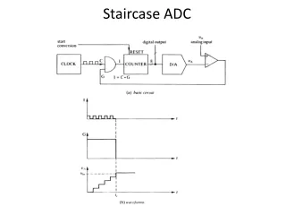
Dual-SlopeIntegrator-Based Design • Switch connects Vin with integrator • Switch held for fixed number of clock cycles • Analog switched at set time to –Vref • T2 clock cycles proportional to Vin • Vin = Vref x T2/T1
Dual-SlopeIntegrator-Based Design Advantages • Insensitive to components value errors • Can achieve high resolution (but at the cost of speed) • Useful for highly accurate measurements Disadvantages • Speed, 2^n-1 clock cycles • Limited applications
Sigma-Delta • Analog signal set to integrator • Resulting “sawtooth” waveform compared with zero volts • Output either high or low Clock rate used is very high, results in “oversampling” of data • Output converted to positive or • negative Vresand fed back to be • added to next sample’s Vin • Resulting stream of 0’s and 1’s • represents the analog signal • average voltage
Sigma-Delta Advantages • High Resolution • No need for precision components Disadvantages • Speed, Oversampling • Only applicable for low bandwidth
Successive Approximation Example Given: 8 bit ADC Vin = 0.2 V Vref = 2 V Find: n bit digital output 2n = 28 = 256 Vres= Vref/ 256 Vres= 0.0078125 V (Resolution)
Successive Approximation Example (cont.) 0.4 < 1 0.4 < 0.5 0.4 > 0.25 0.4 > 0.375 0.4 <0.4375 0.4 <0.4063 0.4 > 0.39 0.4 > 0.398 Digital Output
The ATD10B8C on the MC9S12C32 Input Pins ATD10B8C
The Basics of the ATD10B8C • Resolution: 8- or 10-bit (manually chosen) • 8-channel multiplexed inputs • Successive Approximation architecture • Can perform single or continuous sampling • Can sample single or multiple channels • Conversion time: 7 µs (in 10-bit mode) • Optional external trigger
Single Channel (MULT = 0)Single Conversion (SCAN = 0) ATDDR7 ATDDR6 7 6 5 4 3 2 1 0 ATDDR5 ATDDR4 ATDDR3 Port AD Result Register Interface ATDDR2 ATDDR1 ATD Converter ATDDR0
Single Channel (MULT = 0)Continuous Conversion (SCAN = 1) ATDDR7 ATDDR6 7 6 5 4 3 2 1 0 ATDDR5 ATDDR4 ATDDR3 Port AD Result Register Interface ATDDR2 ATDDR1 ATD Converter ATDDR0
Multiple Channel (MULT = 1)Single Conversion (SCAN = 0) ATDDR7 ATDDR6 7 6 5 4 3 2 1 0 ATDDR5 ATDDR4 ATDDR3 Port AD Result Register Interface ATDDR2 ATDDR1 ATD Converter ATDDR0
Single Channel (MULT = 1)Continuous Conversion (SCAN = 1) ATDDR7 ATDDR6 7 6 5 4 3 2 1 0 ATDDR5 ATDDR4 ATDDR3 Port AD Result Register Interface ATDDR2 ATDDR1 ATD Converter ATDDR0
Left-Justified Result Register • Right-Justified Result Register is similar. • Each register has a high and a low byte. • 8 Result Registers total ($0090 - $009F)
Setting Up the ATD • Step 1: Power-up the ATD and define settings in ATDCTL2 ADPU= 1 powers up the ATD ASCIE = 1 enables interrupt • Step 2: Wait for ATD recovery time (~ 20μs) before proceeding • Step 3: Set the number of successive conversions in ATDCTL3 S1C, S2C, S4C, S8C determine the number of conversions (see Table 8-4)