Download
1 / 29
290 likes | 461 Views
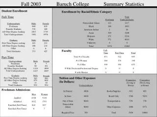
CMPUT329 - Fall 2003. Topic: Internal Organization of an FPGA José Nelson Amaral. Source Material. Xilinx, Spartan II 2.5V FPGA Family: Functional Description, Sept. 2003. Xilinx, Spartan II 2.5V FPGA Family: Introduction and Ordering Information, Sept. 2003.

E N D
CMPUT329 - Fall 2003 Topic: Internal Organization of an FPGA José Nelson Amaral CMPUT 329 - Computer Organization and Architecture II
Source Material Xilinx, Spartan II 2.5V FPGA Family: Functional Description, Sept. 2003 Xilinx, Spartan II 2.5V FPGA Family: Introduction and Ordering Information, Sept. 2003 CMPUT 329 - Computer Organization and Architecture II
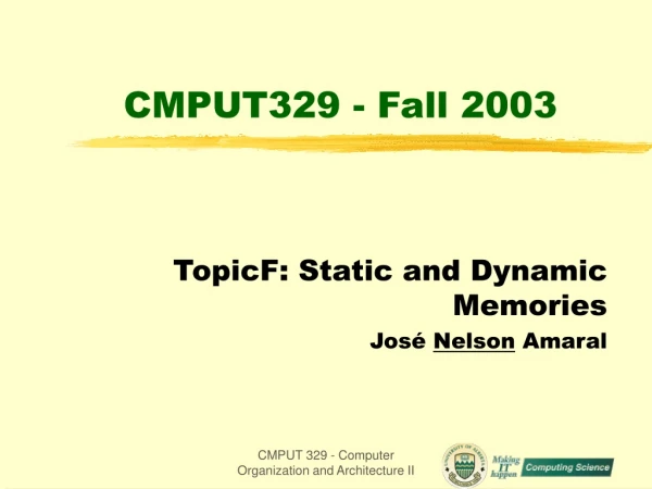
Basic Spartan-II FPGA Block Diagram Configurable Logic Blocks (CLBs) provide the functional elements to implement most of the logic. Delay-Locked Loops (DLLs) distribute the clock and properly compensate for delays. Input/Output Blocks (IOBs) interface between the package pins and the internal logic. Block RAMs each has 4096 bits. CMPUT 329 - Computer Organization and Architecture II
SR SR SR D D D Q Q Q CK CK CK EC EC EC T Package Pin CLK VCC TCE TFF Programmable Bias & ESD Network SR Package Pin O Programmable Output Buffer Internal Reference OCE OFF Programmable Delay IQ I Package Pin Programmable Input Buffer ICE IFF To Next I/O To Other External VREF Inputs of Bank Spartan-II Input/Output Block (IOB)
IOB Registers may be: edge-triggered D-type flip-flops level-sensitive latches T SR Package Pin D Q CLK CK VCC TCE EC TFF Programmable Bias & ESD Network SR Package Pin SR O D Q Programmable Output Buffer CK Internal Reference OCE EC OFF Programmable Delay IQ SR I D Q Package Pin Programmable Input Buffer CK ICE EC IFF To Next I/O To Other External VREF Inputs of Bank Spartan-II Input/Output Block (IOB)
A clock signal is shared by the three registers. T SR Package Pin D Q CLK CK VCC TCE EC TFF Programmable Bias & ESD Network SR Package Pin SR O D Q Programmable Output Buffer CK Internal Reference OCE EC OFF Programmable Delay IQ SR I D Q Package Pin Programmable Input Buffer CK ICE EC IFF To Next I/O To Other External VREF Inputs of Bank Spartan-II Input/Output Block (IOB)
Each register has an independent clock enable. T SR Package Pin D Q CLK CK VCC TCE EC TFF Programmable Bias & ESD Network SR Package Pin SR O D Q Programmable Output Buffer CK Internal Reference OCE EC OFF Programmable Delay IQ SR I D Q Package Pin Programmable Input Buffer CK ICE EC IFF To Next I/O To Other External VREF Inputs of Bank Spartan-II Input/Output Block (IOB)
The three registers share a Set/Reset (SR) line. synchronous Set synchronous Reset asynchronous Preset asynchronous Clear The SR input can be independently configured in each register as: T SR Package Pin D Q CLK CK VCC TCE EC TFF Programmable Bias & ESD Network SR Package Pin SR O D Q Programmable Output Buffer CK Internal Reference OCE EC OFF Programmable Delay IQ SR I D Q Package Pin Programmable Input Buffer CK ICE EC IFF To Next I/O To Other External VREF Inputs of Bank Spartan-II Input/Output Block (IOB)
The I/O buffers and all control signals have independent polarity controls. T SR Package Pin D Q CLK CK VCC TCE EC TFF Programmable Bias & ESD Network SR Package Pin SR O D Q Programmable Output Buffer CK Internal Reference OCE EC OFF Programmable Delay IQ SR I D Q Package Pin Programmable Input Buffer CK ICE EC IFF To Next I/O To Other External VREF Inputs of Bank Spartan-II Input/Output Block (IOB)
Input Path: The IOB routes an input signal either directly or through an optional input flip-flop. T SR Package Pin D Q CLK CK VCC TCE EC TFF Programmable Bias & ESD Network SR Package Pin SR O D Q Programmable Output Buffer CK Internal Reference OCE EC OFF Programmable Delay IQ SR I D Q Package Pin Programmable Input Buffer CK ICE EC IFF To Next I/O To Other External VREF Inputs of Bank Spartan-II Input/Output Block (IOB)
Input Path: The IOB routes an input signal either directly or through an optional input flip-flop. T SR Package Pin D Q CLK CK VCC TCE EC TFF Programmable Bias & ESD Network SR Package Pin SR O D Q Programmable Output Buffer CK Internal Reference OCE EC OFF Programmable Delay IQ SR I D Q Package Pin Programmable Input Buffer CK ICE EC IFF To Next I/O To Other External VREF Inputs of Bank Spartan-II Input/Output Block (IOB)
Input Path: The optional delay eliminates pad-to-pad hold time. The delay matches the internal clock distribution delay of the FPGA, assuring that the pad-to-pad hold time is zero. T SR Package Pin D Q CLK CK VCC TCE EC TFF Programmable Bias & ESD Network SR Package Pin SR O D Q Programmable Output Buffer CK Internal Reference OCE EC OFF Programmable Delay IQ SR I D Q Package Pin Programmable Input Buffer CK ICE EC IFF To Next I/O To Other External VREF Inputs of Bank Spartan-II Input/Output Block (IOB)
SR SR SR D D D Q Q Q CK CK CK EC EC EC Output path: a three-state output buffer drives the signal onto the pad. T Package Pin CLK VCC TCE TFF Programmable Bias & ESD Network SR Package Pin O Programmable Output Buffer Internal Reference OCE OFF Programmable Delay IQ I Package Pin Programmable Input Buffer ICE IFF To Next I/O To Other External VREF Inputs of Bank Spartan-II Input/Output Block (IOB)
SR SR SR D D D Q Q Q CK CK CK EC EC EC Output path: the output signal can be routed directly to the buffer or through an optional IOB output flip-flop. T Package Pin CLK VCC TCE TFF Programmable Bias & ESD Network SR Package Pin O Programmable Output Buffer Internal Reference OCE OFF Programmable Delay IQ I Package Pin Programmable Input Buffer ICE IFF To Next I/O To Other External VREF Inputs of Bank Spartan-II Input/Output Block (IOB)
SR SR D D Q Q CK CK EC EC Output path: the output signal can be routed directly to the buffer or through an optional IOB output flip-flop. T Package Pin CLK VCC TCE TFF Programmable Bias & ESD Network SR Package Pin SR O D Q Programmable Output Buffer CK Internal Reference OCE EC OFF Programmable Delay IQ I Package Pin Programmable Input Buffer ICE IFF To Next I/O To Other External VREF Inputs of Bank Spartan-II Input/Output Block (IOB)
SR SR D D Q Q CK CK EC EC Output path: the three-state control of the output can also be routed directly to the buffer or through an optional IOB output flip-flop. T Package Pin CLK VCC TCE TFF Programmable Bias & ESD Network SR Package Pin SR O D Q Programmable Output Buffer CK Internal Reference OCE EC OFF Programmable Delay IQ I Package Pin Programmable Input Buffer ICE IFF To Next I/O To Other External VREF Inputs of Bank Spartan-II Input/Output Block (IOB)
SR D Q CK EC Output path: the three-state control of the output can also be routed directly to the buffer or through an optional IOB output flip-flop. T SR Package Pin D Q CLK CK VCC TCE EC TFF Programmable Bias & ESD Network SR Package Pin SR O D Q Programmable Output Buffer CK Internal Reference OCE EC OFF Programmable Delay IQ I Package Pin Programmable Input Buffer ICE IFF To Next I/O To Other External VREF Inputs of Bank Spartan-II Input/Output Block (IOB)
SR SR SR D D D Q Q Q CK CK CK EC EC EC All pads are protected against damage from electrostatic discharge (ESD) and from over-voltage transients. T Package Pin CLK VCC TCE TFF Programmable Bias & ESD Network SR Package Pin O Programmable Output Buffer Internal Reference OCE OFF Programmable Delay IQ I Package Pin Programmable Input Buffer ICE IFF To Next I/O To Other External VREF Inputs of Bank Spartan-II Input/Output Block (IOB)
COUT YB Carry and Control Logic Y Look-Up Table G4 S I4 D Q YQ G3 I3 CK O G2 I2 EC G1 I1 R Each slice has two identical logic cells (LC) F5IN BY SR CLK CE XB Carry and Control Logic X Look-Up Table G4 S I4 D Q XQ G3 I3 CK O G2 I2 A Configurable Logic Block (CLB) has two identical slices EC G1 I1 R BX CIN Spartan-II CLB Slice
COUT YB Carry and Control Logic Y Look-Up Table G4 S I4 D Q YQ G3 I3 A logic cell has a 4-input function generator, carry logic and an storage element. CK O G2 I2 EC G1 I1 R F5IN The output from the function generator drives the CLB output and the D input of the flip-flop. BY SR CLK CE XB Carry and Control Logic X Look-Up Table G4 S I4 D Q XQ G3 I3 CK O G2 I2 A CLB also contains logic to combine function generators to provide functions of five or six inputs. EC G1 I1 R BX CIN Spartan-II CLB Slice
Look-Up Tables A Look-Up Table is a 161 RAM. It can be used as a function generator for any logic function with up to 4 Inputs and one output • In the Spartan-II, an LUT can also provide • the functionality of: • a 16 1-bit synchronous RAM • A 16-bit shift register CMPUT 329 - Computer Organization and Architecture II
COUT YB Carry and Control Logic Y Look-Up Table G4 S I4 D Q YQ G3 I3 CK O G2 I2 EC G1 I1 The storage element can be configured as: edge-triggered D flip-flop level-sensitive latch. R F5IN BY SR CLK CE XB Carry and Control Logic X Look-Up Table G4 S I4 D Q XQ G3 I3 CK O G2 I2 EC G1 I1 R BX CIN Spartan-II CLB Slice
COUT YB Carry and Control Logic Y Look-Up Table G4 S I4 D Q YQ G3 I3 CK O G2 I2 EC G1 I1 The D input can be driven by the function generator or directly from the slice inputs. R F5IN BY SR CLK CE XB Carry and Control Logic X Look-Up Table G4 S I4 D Q XQ G3 I3 CK O G2 I2 EC G1 I1 R BX CIN Spartan-II CLB Slice
COUT YB Carry and Control Logic Y Look-Up Table G4 S I4 D Q YQ G3 I3 CK O G2 I2 EC G1 I1 The D input can be driven by the function generator or directly from the slice inputs. R F5IN BY SR CLK CE XB Carry and Control Logic X Look-Up Table G4 S I4 D Q XQ G3 I3 CK O G2 I2 EC G1 I1 R BX CIN Spartan-II CLB Slice
COUT YB Carry and Control Logic Y Look-Up Table G4 S I4 D Q YQ G3 I3 CK O G2 I2 EC G1 I1 R The FF receive the same clock signal. F5IN BY SR CLK CE XB Carry and Control Logic X Look-Up Table G4 S I4 D Q XQ G3 I3 CK O G2 I2 EC G1 I1 R BX CIN Spartan-II CLB Slice
COUT YB Carry and Control Logic Y Look-Up Table G4 S I4 D Q YQ G3 I3 CK O G2 I2 EC G1 I1 R Each slice has synchronous set and reset signals F5IN BY SR SR forces a storage element into the initialization state specified for it in the configuration CLK CE XB Carry and Control Logic X Look-Up Table G4 S I4 D Q XQ G3 I3 CK O G2 I2 EC G1 I1 R BX CIN Spartan-II CLB Slice
COUT YB Carry and Control Logic Y Look-Up Table G4 S I4 D Q YQ G3 I3 CK O G2 I2 EC G1 I1 R Each slice has synchronous set and reset signals F5IN BY SR SR forces a storage element into the initialization state specified for it in the configuration CLK CE XB Carry and Control Logic X Look-Up Table G4 S I4 D Q XQ G3 I3 CK O G2 I2 BY forces it into the opposite state. EC G1 I1 R BX CIN Spartan-II CLB Slice SR and BY can be configured to work asynchronously.
Basic Spartan-II FPGA Block Diagram Configurable Logic Blocks (CLBs) provide the functional elements to implement most of the logic. Delay-Locked Loops (DLLs) distribute the clock and properly compensate for delays. Input/Output Blocks (IOBs) interface between the package pins and the internal logic. Block RAMs each has 4096 bits. CMPUT 329 - Computer Organization and Architecture II