Download
1 / 19
190 likes | 219 Views
Delve into the realm of optoelectronics and solid-state physics, exploring elemental and compound semiconductors, crystal structures, band diagrams, and bonding in solids. Learn about dislocations, strains, crystal growth methods such as epitaxy, and doping of semiconductors. Discover the significance of energy band theory and optical fiber technology in this comprehensive guide.

E N D
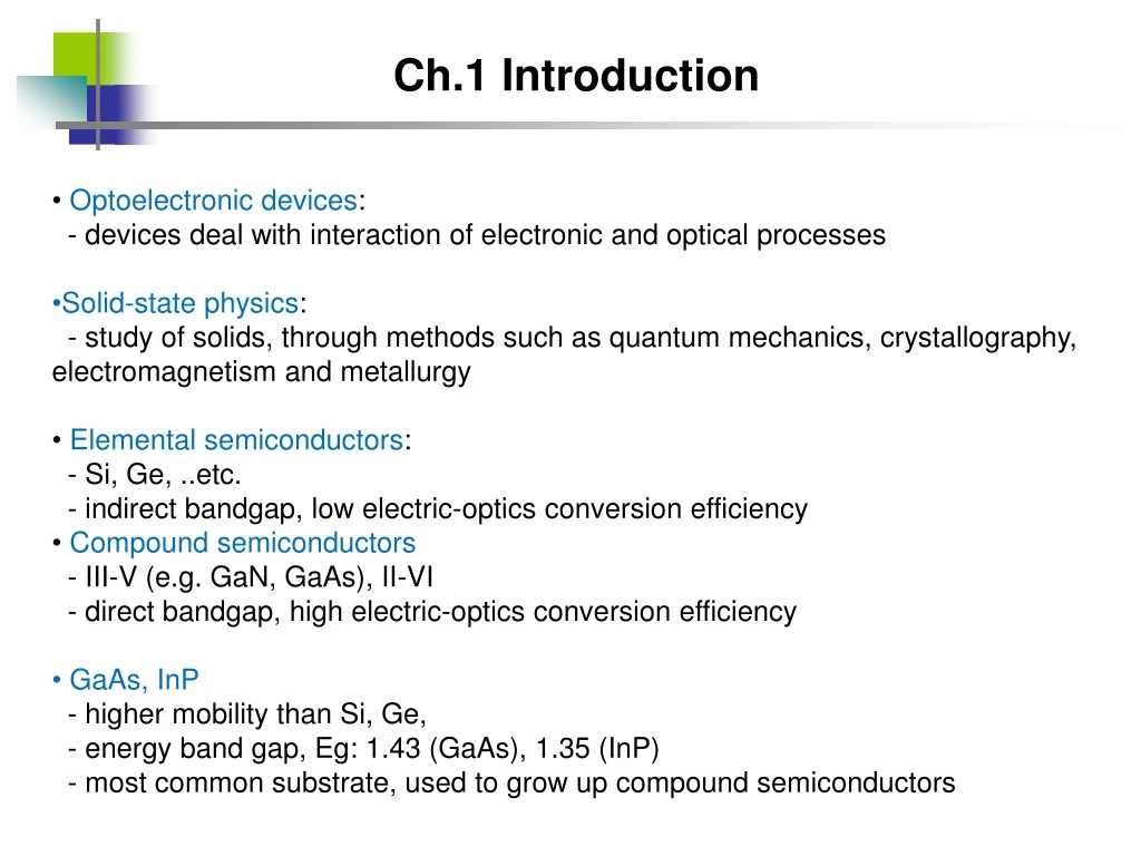
Ch.1 Introduction • Optoelectronic devices: • - devices deal with interaction of electronic and optical processes • Solid-state physics: • - study of solids, through methods such as quantum mechanics, crystallography, electromagnetism and metallurgy • Elemental semiconductors: • - Si, Ge, ..etc. • - indirect bandgap, low electric-optics conversion efficiency • Compound semiconductors • -III-V (e.g. GaN, GaAs), II-VI • -direct bandgap, high electric-optics conversion efficiency • GaAs, InP • - higher mobility than Si, Ge, • - energy band gap, Eg: 1.43 (GaAs), 1.35 (InP) • - most common substrate, used to grow up compound semiconductors
Band structure • Band structure: • - results of crystal potential that originates from equilibrium arrangement of atoms • in lattice - directed from potential model and electron wave equation (Schrodinger equation) time-dependent Schrodinger equation E: electron energy, φ:wave equation, m: electron mass, ħ: Plank constant
Bonding in solids • Van der Waals bonding: formation of dipoles between atoms and their electrons e.g.: inert gas, like Ar • Ionic bonding: electron exchange between atoms produces positive and negative ions which attract each other by Coulomb-type interactions e.g. NaCl, KCl • covalent bonding sharing of electrons between neighboring atoms e.g.: elemental and compound semiconductors • Metallic bonding: valence electrons are shared by many atoms (bonding not directional, electron free or nearly free contributed to conductivity) e.g.: Zn
Body-Centered Cubic (BCC) structure http://stokes.byu.edu/bcc.htm e.g. iron, chromium, tungsten, niobium
Face-Centered Cubic (FCC) structure e.g.: aluminum, copper, gold, silver http://stokes.byu.edu/fcc.htm
Diamond Cubic (FCC) structure http://zh.wikipedia.org/zh-tw/File:Diamond_Cubic-F_lattice_animation.gif
Zincblende structure • Diamond structure, Zincblende structure e.g.: Si, Ge e.g.: aluminum, GaAs
Dislocation & strain • Dislocationoccurs if - epitaxial layer thickness > hc (critical thickness), or - epitaxial layer thickness < hc, but with large mismatch • Strain occurs if - epitaxial layer thickness < hc, and with small mismatch
Strain semiconductor • a) lattice match b) compressive strain c) tensile strain • Strain offer flexibility for restriction of lattice mismatch
Crystal Growth • Bulk growth: - furnace growth - pulling technique • Epitaxial growth: - Liquid Phase Epitaxy (LPE) - Vapor Phase Epitaxy (VPE), or termed Chemical Vapor Deposition (CVD) - Molecular Beam Epitaxy (MBE)
Epitaxy • epi means “above” taxis means “in order manner” epitaxy can be translated to “to arrange upon” • with controlled thickness and doping • subtract acts as a seed crystal, deposited film takes on a lattice structure and orientation identical to the subtract • different from thin film deposition that deposit polycrystalline or amorphous film • - homoepitaxy: epi and subtract are with the same material • epi layer more pure than subtract and have different doping level - hetroepitaxy: • used for - Si-based process for BJT and CMOS, or - compound semiconductors, such as GaAs
Epitaxy Material Growth Methods • Liquid Phase Epitaxy • Vapor Phase Epitaxy (VPE), or termed Chemical Vapor Deposition (CVD) - formation of condensed phase from gas of different chemical composition - distinct from physical vapor deposition (PVD) such as sputtering, e-beam deposition, MBE (condensation occurs without chemical change) - gas stream through a reactor and interact on a heated subtract to grow epi layer • Molecular Beam Epitaxy
Doping of Semiconductors • Intrinsic materials:undoped • - Undoped materials by epitaxy technology have more carriers than in intrinsic • material. e.g. GaAs: 1013 /cm3 (instrinsic carrier concentration: 1.8x10⁶ /cm3) • - impurity comes from source materials, carrier gases, process equipment, or • subtract handle • Extrinsic materials: • - n-type: III sub-lattice of III-V compound is substituted by V elements: impurity terms “donor” • - p-type: V sub-lattice of III-V compound is substituted by III elements: impurity terms “acceptor” http://www.siliconfareast.com/sigegaas.htm
Optical fiber - lowest loss at 1.55 um - lowest dispersion” 1.3 um