Download

1 / 14
150 likes | 499 Views
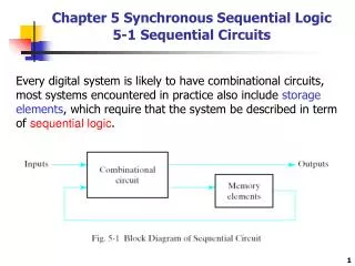
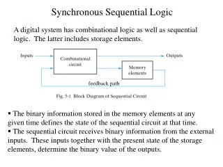
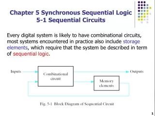
Synchronous Sequential Logic. A digital system has combinational logic as well as sequential logic. The latter includes storage elements. feedback path. The binary information stored in the memory elements at any given time defines the state of the sequential circuit at that time.

E N D
Synchronous Sequential Logic A digital system has combinational logic as well as sequential logic. The latter includes storage elements. feedback path • The binary information stored in the memory elements at any given time defines the state of the sequential circuit at that time. • The sequential circuit receives binary information from the external inputs. These inputs together with the present state of the storage elements, determine the binary value of the outputs.
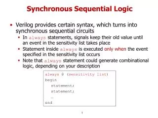
Synchronous Sequential Logic • A synchronous sequential circuit employs signal that affect the • storage elements only at discrete instants of time. • Synchronization is achieved by a time device called clock • generator that provides a periodic train of clock pulses. • Storage elements that are used in clocked sequential circuits • are called flip-flops. • A flip flop is a a binary storage device capable of storing one • bit of information.
Synchronous Clocked Sequential Logic The outputs can come either from the combinational circuit or from the flip-flops or both. The flip-flops receive their inputs from the combinational circuit and a clock signal. The state of the flip-flops can change only during a clock pulse transition.
LATCHES The most basic types of flip-flops are the latches that operate with signal levels. Latches are the building blocks of all flip-flops. undefined state Under normal conditions, both inputs of the latch remain 0 unless the state has to be changed. When S = 1 latch to ‘set’ state: Q = 1, Q’ = 0. Before R is reset to 1, S must go back to 0 to avoid the occurrence of an undefined state with both outputs = 0
SR LATCH with NAND undefined state • SR latch with NAND gates requires a 0 signal to change its state. • The inputs signals for the NAND-latch are the complement values • used for the NOR latch.
SR LATCH with Control Input • The control input C determines when the state of the latch can • be changed. • When C = 0, the output of the NAND gates stays at 1 No change • in state. • When S = 1, R = 0, C = 1 ‘set’ state • When S = 0, R = 0, C = 1 no change in state • When S = 0, R = 1, C = 1 ‘reset’ state
D LATCH D latch eliminates the undesirable condition of the indeterminate state that occurs in the SR latch (Q = Q’ = 1). If D = 1, Q= 1 ‘set’ state If D = 0, Q= 0 ‘reset’ state
Flip-Flops • A flip-flop is a state of a latch that can be switched by momentary • change in the control input. • This momentary change is called a trigger and the transition it causes • is said to trigger the flip-flop. • The D-latch is a flip-flop that is triggered every time the pulse goes • to a high or logic level 1. • As long as the input pulse remains at this level, any changes in the • input data will cause a change in the output and the state of the latch.
Edge-Triggered Flip-Flop The circuit samples the D input and changes its output at the negative edge of the clock, CLK. When the clock is 0, the output of the inverter is 1. The slave latch is enabled and its output Q is equal to the master output Y. The master latch is disabled (CLK = 0). When the CLK changes to high, D input is transferred to the master latch. The slave remains disabled as long as C is low. Any change in the input changes Y, but not Q. The output of the flip-flop can change when CLK makes a transition 1 0
Positive-Edge-Triggered Flip-Flop • If D = 0 when CLKR 0, Q = 0: ‘reset state’ • If D changes while CLK is high flip-flop will not respond to the change. • When CLK , R1, flip-flop will be in the same state (no change in output). • If D = 1 when CLK , S 0, Q = 1: ‘set state’
Edge-Triggered Flip-Flop: Graphic Symbols The most economical and efficient flip-flop constructed is the edge-triggered D flip-flop since it requires the smallest number of gates.
JK Flip-Flop • JK flip-flop is capable of performing: set to 1, reset to 0, or • complementing its output: • The J input sets the flip-flop to 1. • The K input resets the flip-flop to 0. • When J and K are enabled, the output is complemented.
JK Flip-Flop When J = 1 and K = 0, D = 1 next clock edge sets output to 1. When J = 0 and K = 1, D = 0 next clock edge resets output to 0. When J = 1 and K = 1, D = Q’ next clock edge complements output. When J = 0 and K = 0, D = Q next clock edge leaves output unchanged.