Download
1 / 16
160 likes | 168 Views
This presentation provides an updated status on the hardware and FPGA firmware of the Baby-Mind SiPM front-end electronics. It includes information on the hardware status, FPGA firmware status, measurements, and the conclusion.

E N D
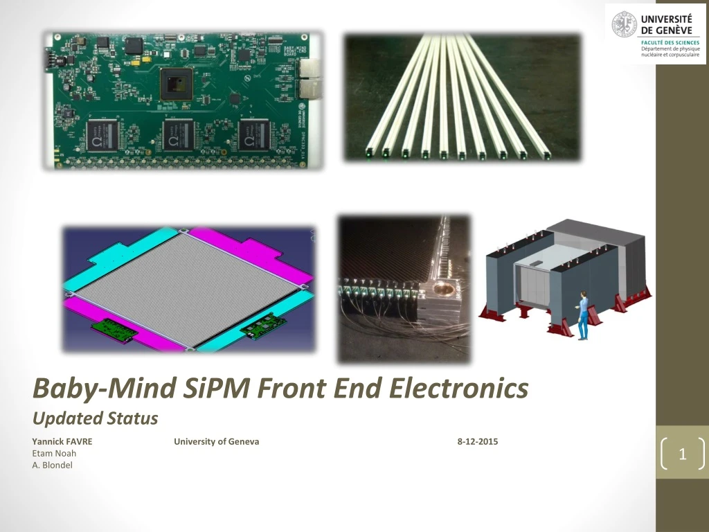
Baby-Mind SiPM Front End Electronics Updated Status Yannick FAVRE University of Geneva 8-12-2015 Etam Noah A. Blondel
OUTLINE • Hardware status • FPGA firmware status • Measurements • Status & Conclusion
Hardware Status Current Board :1 board under test • LV Power supplies : OK • FPGA programming : OK • USB µC & interface : OK • ASIC : • Slow control • HV DAC : OK • Fast Internal Triggers & OR32 : OK • Fast Internal Triggers OUT: TB Tested • Preamp, Shaper, Hold, Mux OUT LG/HG : OK • ADC : OK • ADC signal conditioning : TB Modified • ASIC baseline subtraction + gain change for best ADC resolution % ASIC output • HV : TBT • Gigabit : TBT • 4 board to be started-up for tests with SiPM
FPGA FIRMWARE ALTERA ARIA5 (BGA896) A7 on proto, A3 or A5 on production - Code : Quartus dev. tool, VHDL behavorial (design reuse) + some FPGA IP specific modules
FPGA FIRMWARE STATUS • FullysimulatedwithModelsim • Tested on Hardware + USB communication
Measurements • Configuration: • 84-channels enabled over 96 (28CH/ASIC) • 1 channel / ASIC connected to calibration input : HG/LG CTest enabled on CH0, CH29, CH60 • HG gain=40, LG gain = 30 • Time constant = 87.5ns, FPGA HOLD optimized for shaper peak (175ns) • Fast shaper on LG, OR32 output & DAC10b=300 • 96-CH LG+HG Mux readout @ ~10us (1/4MHz x 32-ch + 2µs latency) • External Generator : Square 0/100mV 5KHz on ASIC calibration input • 2 DAQ modes within FPGA: • Compare: • Triggered by 3xOR32 from ASICs • Use HOLD signal to latch analog signal on shaper peak • Each channel can be compared to baseline computed + user threshold and sent to readout • Compute: • Free running when not in compare mode • No hold signal • Used for independent CH baseline computation (Low Pass filter)
Measurements Compute (1024 samples) ASIC 0 CH0 to CH27 Compare (51 samples =1024*5KHz*10us)
Measurementssynthesis : 84 CH Channels on Generator CH60 CH29 CH0 <1 LSB on LG non excited CH <2 LSB on LG excited CH <2 LSB on HG non excitedCH <5 LSB on HG excitedCH Used for baseline computation ASIC2 ASIC1 ASIC0
STATUS & CONCLUSION • Current board Hardware : • ASIC analog signals conditioning modification & tests : ~2weeks • SiPM simple tests: mid January • 4 boards to be started : mid January • HV & independent ASIC trigger tests : End January • FPGA size validation, power consumption, Gigabit links : TBD • Current board FPGA firmware : • 1st version : Analog (No timing, No baseline computation within FPGA) : ~2weeks • 2nd version : Analog + baseline computation within FPGA : mid January • 3rd version : Analog + Timing : End January • 4th version : Analog + Timing + USB multi-board chain : TBD vs Hardware • 5thversion : Analog + Timing + USB or Gigabit multi-board chain : TBD • Next Hardware : Design start end of January • ASIC analog signals conditioning • Trigger chain • FPGA remote FW update • Ethernet/Optic link ? • ASIC input protection • Analog input connectors stage • STILL NEED A SOFTWARE ENGINEER FOR: • USB real time optimisation • Labview interface • DLL access & Scripting command run • Software finalization + graphs
FRONT-END BOARD • 96 coax. connectors (84 used) • 3 CITIROC ASICs 32-ch • 12-bits 8-ch 40Ms/s/ch ADC • Altera ARIA5 FPGA : • Timing : 2.5ns resolution • Analog : 8µs for 96-ch LGain & HGain • HV, ASIC T° + board T° + RH% • Readout/Slow control on USB3 and/or Gigabit RJ45 chain • External propagated Trig/sync. Signal • Power supplies (HV/LV) 240 24V LVs USB RJ45 FPGA ADC HV 130 ASICs 96 coax. (top/bot) FEB prototype
READOUT & SLOW CONTROL – CABLING OPTIONS - Number of chained FEB depends on events frequency and bandwidth limit => application specific - Ex : 8 chained FEB for Baby-Mind (VRB limitation)
READOUT – USB3 software Readout & general tab • C# Win7 (ms visual studio) • Versatile architecture designed for reuse: • Low level classes for protocol communication handling • Hardware slow control direct building & mapping through abstraction classes • Direct connection to FPGA/ASIC trough USB3 • Simple building & hardware mapping • File handling (HML open/save File) • Ex : myBoard.myAsic[0].addVar(Type, Name, DefaultVal, Min, Max, BitLocation…) • GUI direct connection with slow control variables declared from abstraction classes : • Simple building • Automatic coherency check (Min, Max) • Ex : boolean connected to a checkBox, Byte connected to a textBox … • Readout Save to file: • 2.5Gb/s to 3Gb/s achieved from USB3 • Some problems to be solved at low speed (low event frequency) • Linux planned & Labview virtual instrument ASIC0 slow control tab
Protocol Readout Slow Control