Download
1 / 11
110 likes | 260 Views
Vertex Readout. Joel Goldstein PPd, RAL 4 th ECFA/DESY LC Workshop DAQ Session 1 st April 2003. Vertex detector conceptual design CP CCD technology option Planned readout scheme Other scenarios (More demanding TESLA environment used throughout). Outline. The Vertex Detector.

E N D
Vertex Readout Joel Goldstein PPd, RAL 4th ECFA/DESY LC Workshop DAQ Session 1st April 2003
Vertex detector conceptual design CP CCD technology option Planned readout scheme Other scenarios (More demanding TESLA environment used throughout) Outline
The Vertex Detector • 5 layers (15-60mm) • ~ 0.1% X0 per layer • 20 m 20 m pixels • 800 million channels • Background rates force readout • 50 s for Layer 1 • 250 s for Layer 2
Separate readout for each column Readout chip bump-bonded to CCD Chips contain: Amplifiers 5-bit FADCs Filters Sparsification logic Local memory Column Parallel CCDs
Layer 1 read out 20 times per bunch train 50k z pixels Layer 2 read out 5 times per bunch train 31k z pixels 31 bits/4 bytes pixel address Ladder Readout
4.4 billion pixels 5 bits = a lot of data! So, Sparsify locally into clusters (22,…) Store on chip Readout during 200ms dead time 1.3 million hits = 20 Mbytes per bunch train DAQ Plan
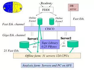
Detector Level DAQ
NLC: Bkgd hits/train ~ 0.1TESLA Readout in 8.3 ms dead time TESLA 800: 2bunches/train Same CCD clock speed More capacity in readout? Memory, datalinks etc. Still to be looked at Active Pixels: Similar schemes feasible Other Scenarios
800 MPixel CP CCD vertex detector Clustering and sparsification performed on readout chip ~10 Mbytes per bunch train per end Single interface card per end, outside tracking volume Minimal external connections input control fibre, output data fibre, power Other technologies similar Testing of first CP CCDs and readout chips starting Summary