Download
1 / 11
120 likes | 262 Views
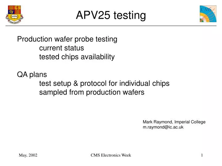
APV25 testing. Production wafer probe testing current status tested chips availability QA plans test setup & protocol for individual chips sampled from production wafers. Mark Raymond, Imperial College m.raymond@ic.ac.uk. APV25 wafer testing status.

E N D
APV25 testing Production wafer probe testing current status tested chips availability QA plans test setup & protocol for individual chips sampled from production wafers Mark Raymond, Imperial College m.raymond@ic.ac.uk CMS Electronics Week
APV25 wafer testing status first 10 engineering wafers (September, 2000) all diced, ~1300 KGD still available at IC 2 production wafer lots delivered January: 48 ordered, 24 + 21 = 45 delivered shortfall of 3 (rejected by manufacturer QA) processing problem – these 2 lots being replaced 3rd full lot launched to provide remaining 3 (25 wafers/lot) 3 wafers delivered mid Feb. remaining 22 requested and delivered early March back to high yield, 13 wafers now diced CMS Electronics Week
Results from 1st 2 production lots Lot 1 -> low yield (17 – 36 %) some good chips around periphery circular area of good chips in centre ~ even split between digital and analogue failure modes Lot 2 -> lower yield (1 – 21 %) similar circular pattern but no good chips in centre manufacturer notified via CERN (F.Faccio) investigation launched early acknowledgement of likely process problem example wafers returned and investigated problem traced to silicide layer (gate/source/drain contact layer) these lots being replaced CMS Electronics Week
Results from 3rd production lot average yield 79% some wafers -> v. high yield others good but still show pattern 36 chips in incomplete reticles now excluded from yield calculation (previously not the case) 94% 73% CMS Electronics Week
Incomplete reticles any reticle within ~ 3mm of wafer edge not completely processed (via layers omitted) penalty for us due to chip grouping (4 APVs/reticle) CMS Electronics Week
Tested chip availability present chip (KGD) availability 1300 remaining chips from engineering run 3800 13 wafers diced from 3rd lot 5100 in waffle packs now + 3300 KGD on remaining uncut 3rd lot wafers 8400 currently in-hand near future 3 wafer lots launched to replace 1st two and investigate problems already passed silicide steps with no problem observed 1st lot now delivered all 3 lots should yield further ~ 20,000 KGD CMS Electronics Week
QA plans wafer probe data stored for each individual chip (pulse shapes, channel pedestals, pipeline pedestals, currents, rough noise estimate, …) wafer test limited by: time (throughput) ~ 1 min/chip environment electrically noisy no close decoupling => more detailed QA tests performed on chips sampled from each wafer (1/wafer) mounted in custom setup CMS Electronics Week
QA measurement setup APV mounted on simple daughter board 4 inputs bonded allows external charge injection and external capacitance QA plan (IC & Padova) perform detailed tests on 1 chip/wafer irradiate & repeat tests on reduced sample start with high rate, reduce as confidence builds to 20% level (~ 6 wafers/lot) anneal & repeat automated test protocol includes pulse shape tuning (to ideal 50 ns CR-RC) gain & linearity measurements noise (baseline & added capacitance) internal calibration CMS Electronics Week
QA measurement: pre-rad CMS Electronics Week
QA measurement: after 10 Mrads CMS Electronics Week
Conclusions Wafer probing process problems with first two production lots wafers now returned and replacements arriving communication channel (via CERN) to manufacturer effective manufacturer’s response very constructive and helpful throughout 3rd lot yield back at expected high level (average 79%) ~8400 KGD in-hand, 3 more lots available -> ~ 20,000 more in ~ few months More detailed QA measurements automated measurement protocol developed chips sampled from 1st 10 (engineering) wafers all irradiated (10 Mrads) no problems (detailed analysis underway) measurements on chips from 1st production lot about to start irradiation plans for ~ 50% of this lot CMS Electronics Week