Download
1 / 48
480 likes | 651 Views
Thermal and Layout considerations for Integrated FET chargers. Charles Mauney October 2013. Agenda. Why this Topic? PCB Electrical Characteristics DC Parasitics (Resistance) AC Parasitics Grounds and Grounding PCB Thermal Characteristics Conduction Concepts Convection Concepts

E N D
Thermal and Layout considerations for Integrated FET chargers Charles Mauney October 2013
Agenda Why this Topic? PCB Electrical Characteristics DC Parasitics (Resistance) AC Parasitics Grounds and Grounding PCB Thermal Characteristics Conduction Concepts Convection Concepts Examples Common “Poor” Thermal Layouts Good Thermal Layout Good Electrical Layout
Why this Topic? What design component is most often Overlooked? PCB Design • PCB is as critical as any other component • Use the same care with the design of the PCB as other designers take with designing the IC and FET switches Why is layout Important? • Placement of Components effects connection impedance • Ground Plane design affects connection impedance • Electrical/thermal impedance affects current and heat flow • AC Current across impedance causes noise • Heat flow across thermal impedance causes temperature rise
Agenda Why this Topic? PCB Electrical Characteristics • DC Parasitics (Resistance) • AC Parasitics • Grounds and Grounding PCB Thermal Characteristics • Conduction Concepts • Convection Concepts Examples • Common “Poor” Thermal Layouts • Good Thermal Layout • Good Electrical Layout
Copper is Good, but Not a Perfect Conductor Optimizing Placement, Copper Thickness & Routing impacts Regulation Transient Response Efficiency Temperature rise Noise immunity
Metals are good ConductorsSome better than others – ρ(Ω-length) t w
Count Squares to Estimate Trace Resistance Copper resistivity is 0.67 mW in. at 25°C and doubles for 254°C rise
Vias Have Resistance Too Typical rule of thumb is 1 A to 3 A per via
Agenda Why this Topic? PCB Electrical Characteristics DC Parasitics (Resistance) AC Parasitics Grounds and Grounding PCB Thermal Characteristics Conduction Concepts Convection Concepts Examples Common “Poor” Thermal Layouts Good Thermal Layout Good Electrical Layout
Self Inductance of PWB Traces Due to the natural logarithmic relationship, large changes in conductor width have minimal impact on inductance
PWB Traces Over Ground Planes Substantial inductance reduction Inductance inversely proportional to width
Leakage Inductance in AC (Pulsed) Circuits Matters – How much inductance is in a 3” wire? • HP 4275A LCR meter – Sample tested at 1MHz • Shows 79nH for this loop of wire
Inductance – Think again! PCB with copper on bottom Placed next to loop AC current in loop generates opposing currents in copper plane to partially cancel inductance PCB with copper on top Placed next to loop Same Loop area with PCB, copper on bottom; <L Wire loop area reduced; <L PCBwith copper on top; <L
Leakage Inductance – 3” Wire cont’ PCB with copper on top helps just a bit. PCB with copper on bottom added but loop does not produce much of a field to cancel inductance Wire loop twisted – Reversing of current cancels inductance; <L • Loop area and length determine inductance • Leakage Inductance (Parasitic) becomes charged with current • When Current is abruptly stopped – Leakage inductance’s voltage flips polarity and discharges energy typically as noise
Sample Capacitance Calculation Consider two 10 mil traces crossing with 10 mil PWB thickness Capacitance is additive with multiple connected pads
Chaos Created by Noise Injection Ten 0.05 x 0.02 in2 pads in summing junction can increase parasitic capacitance to 2 pF Keep high impedance node area small and away from switching waveforms – above clean ground
Bypass Capacitor Layout Minimize lead inductance Short lengths Minimizes loop area Use ground planes where possible Bring current path across capacitor terminals Parallel different capacitor types Reduced impedance across a frequency band Parallel different ceramic capacitors values and sizes Reduce impedance in the 2-20 MHz frequency range (0.1 mF & 0.01 mF) Use experienced Layout Person Understands Circuit Operation and Layout concepts.
Capacitors Are Inductive… Above Their Self-Resonant Frequency Measured ESL correlates well with rule of thumb inductance of 15 nH/inch High frequency converters use Ceramic caps of different values (10u, 1u, 0.1uF) for low impedance (low inductance) in MHz range.
And Inductors Turn Into Capacitors Inductive at low frequency High frequency, distributed capacitance and mrreduction Maximize inductance by choosing inductor with resonance above “switching edge” frequencies Chip Inductor Wire wound inductor
Other Circuit Effects of Layout Impedances VIN VOUT VIN+ • Good ground plane • Small high frequency current loop • Parasitics, LL, are reduce with integrated FETS • Small area for high dv/dt node QH CIN L LL L VIN- LL QL CIN QH COUT1 CO QL RS COUT2 VOUT- VOUT+
Connect Power Components Properly Draw schematic to reflect desired location relative to other components. Understand circuit operation and AC currents A pulses current is a noise signal – return this current to its source in smallest distance (loop area) – Loop area is antenna. Place power stage to minimize connection impedance Consider two sided mounting, FET’s one side, cap other Use full ground planes to produce low impedance ground connection Use VIAs to connect all component grounds to ground plane – Minimizes return impedance. • Any inductance in di/dt path results in ringing on switched node • Proper design can eliminate need for snubber
Watch Out for Parasitic Components Wiring inductance Added “parasitic” inductance raises impedance of low impedance circuits (filters, power switching) making them less effective. Use wide conductors and ground planes to minimize impedance Board capacitance Allows path for AC signals Good if part of design; Bad when coupling “noise” into sensitive circuits. High impedance nodes are susceptible to switching waveforms. Magnetic coupling Loop to loop, minimize loop areas, use ground planes
Agenda Why this Topic? PCB Electrical Characteristics DC Parasitics (Resistance) AC Parasitics Grounds and Grounding PCB Thermal Characteristics Conduction Concepts Convection Concepts Examples Common “Poor” Thermal Layouts Good Thermal Layout Good Electrical Layout
Single Point Grounds Series Simple wiring – one layer Common impedance causes different potentials High impedance at high frequency (>10 kHz) Parallel Complicated wiring – one layer Reduced differential potentials at low frequencies High impedance at high frequency (>10 kHz)
Multipoint Grounding Ground plane provides low impedance between circuits to minimize potential differences Also, reduces inductance of circuit traces Goal is to contain high frequency currents in individual circuits and keep out of ground plane Segregated circuits No current between Circuits No current No ground noise shared between circuits, V=IR
Agenda Why this Topic? PCB Electrical Characteristics DC Parasitics (Resistance) AC Parasitics Grounds and Grounding PCB Thermal Characteristics Conduction Concepts Convection Concepts Examples Common “Poor” Thermal Layouts Good Thermal Layout Good Electrical Layout
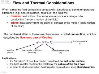
Modeling Temperature Rise Rjc: Junction to Case (PWRPAD of IC), thermalresistance (ºC/W) Rcs: Case to Heat Sink (PWRPAD-IC to PWRPAD-PCB), thermal resistance Rsa: Sink (PCB surface) to ambient resistance • Heat is conducted through device base into circuit board • It spreads laterally through copper conductors • Final path is convection cooling from board surface to ambient
Thermal Conductivity of Other Materials • Thermal Conductivity is in the denominator • Thus a large value is good for a low thermal impedance. • Silver is slightly better than copper but costs too much • FR4 (Epoxy) is very poor.
Thermal Resistance A single via has about 100°C/W thermal resistance and they can be paralleled • Multiple VIAs will reduce the thermal resistance proportionally • 10VIAs would be 10C/W
Lateral Heat Flow • A square of 2oz copper with 1W of heat applied will result in a 40C rise, R = 40C/W • A square of 0.060” thick FR4 with 1W of heat applied will result in a 2400C rise, R = 2400C/W • Only copper spreads out heat
Thermal Resistance Gap Copper plane has cut out due to routing a signal. Thermal resistance gap significantly adds to temperature rise R = 23C/W for 10mil gap of FR4 R = 0.018 C/W for 10mil gap of Cu • Cutting the Cu plane added • (23C/W – 0.018C/W = 23C/W)
Thermal Resistance for FR4 Through board is much less than board-ambient • 1W applied to 0.125 in sq, 0.060” thick, FR4 (IC area) has temp rise of 548C • 1W applied to 1in sq, 0.06” thick, FR4 has a temp rise of 8C. • FR4 ok for thermally conductivity through large areas. • Poor through small area - IC power pad (need VIAs) or cross-section of PCB.
Agenda Why this Topic? PCB Electrical Characteristics DC Parasitics (Resistance) AC Parasitics Grounds and Grounding PCB Thermal Characteristics Conduction Concepts Convection Concepts Examples Common “Poor” Thermal Layouts Good Thermal Layout Good Electrical Layout
Convection Cooling h - heat transfer coefficient ~0.006 W/in2/°C, 0.001 W/cm2/°C for air 1 W/1in2 =166°C rise; 1 W/cm2 = 1000°C rise Equation for the nonlinearity of h in2 cm2 in2 cm2
Typical Thermal Requirements Ambient temperature: 70°C, TA Maximum semiconductor: 125°C, Max TJ Maximum board temperature: 120°C Typical semiconductor loss: 2 W PowerPAD™ SO-8 thermal resistance: 2.3°C/W Calculated PWB temperature under semiconductor is 125°C – (2 W x 2.3°C/W) = 120°C Allowed PCB Temp Allowed Temperature Rise of PCB = 120°C – 70°C = 50°C
Convection Cooling Area Calculations Solving for Surface Area, for 2W dissipation & a 50°C rise in2 in2 cm2 cm2 • The component heat-sink (PWRPAD) is much smaller than the required cooling area 7 in2, so a heat sink or PCB copper plane has to be used (~2 in2 PCB).
Dissipation on Double-Sided Board 2 W of point source dissipation on double-sided board calculates to ~30°C rise under the source Radius From Heat Source (cm) Radius From Heat Source (inches) • Shown is ~ 33C rise for a 2.5”x2.5” PCB x 2 sides or 12.5in2
Even a Whisper of Air can Reduce Temperatures System airflow yields 20% to 60% drop in temperature rise Metric English
PWB Cooling Strategy Temperature Rise is a FCN of power dissipate divided by surface area; Low Temp Rise PSMALL/ALARGE = dTSMALL Use thick copper, 2oz, to spread heat to larger area. Use multiple common planes on different layers connected by vias Internal Copper Planes are as effective as surface planes for spreading heat, but has temp rise through FR4 Very little penalty once heat is spread out. Use both side to cool Avoid breaks in planes as they substantially degrade lateral heat flow Reduce Area
Agenda Why this Topic? PCB Electrical Characteristics DC Parasitics (Resistance) AC Parasitics Grounds and Grounding PCB Thermal Characteristics Conduction Concepts Convection Concepts Examples Common “Poor” Thermal Layouts Good Thermal Layout Good Electrical Layout
Top and Bottom Layers – Poor Thermal Design Top Layer – Quad bqIC is isolated from top copper plane – No Conduction of heat Bottom Layer – bqIC PWR-PAD vias connected to bottom plane, but area is cut away due to a cutout, parts and Cu pours. Result is limited cooling area.
Two Inner Layers 1st Inner Layer – bqIC PWR-PAD vias connected to plane. Plane is very small due to Routing, vias. Result is limited cooling. 2nd Inner Layer – bqIC PWR-PAD vias connected to plane. Plane is very small due to Routing on all sides. Result is limited cooling.
2 Layer bqIC Layout – Good Layout Bottom Layer – bqIC PWR-PAD vias connected to bottom plane. Best thermal layout – heat from vias can flow in all directions on bottom plane Top Layer – Quad bqIC is isolated from top copper plane
EVM Thermal Plot – 2.23W Dissipated1”x2” 2 Layer, 2oz Cu, 0.031” Thick PCB • Boost Converter –Top Layer • Vbatin=3.3V, 5Vout, Iout=2.12A, • 1) IC, 2) Inductor, 3) PCB, 4) Edge of PCB Boost Converter – Bottom Layer Vbatin=3.3V, 5Vout, Iout=2.12A, 1) IC, 2) Whole PCB, 3) Ambient, 4) ~1”sq Center
EVM Thermal Plot – 0.71W Dissipated 1”x2” 2 Layer, 2oz Cu, 0.031” Thick PCB • Boost Converter –Top Layer • Vbatin=3.3V, 5Vout, Iout=1A, • 1) IC, 2) Inductor, 3) PCB, 4) Edge of PCB Boost Converter – Bottom Layer Vbatin=3.3V, 5Vout, Iout=1A, 1) IC, 2) Whole PCB, 3) Ambient, 4) ~1”sq Center
Electrical and Thermal Layout Summary • Place components to minimize inductive loops • Understand circuit operation • Keep loop area small for high frequency, di/dt, signals and away from high impedance circuits (Magnetic coupling) • Keep high dV/dt signal’s area small and away from high impedance circuits (Electric Coupling) • Use ground planes to lower over all impedance of the ground plane, thus reducing noise. • Identify hot components and make sure there is a at least one 2oz copper plane to remove heat, >1.5” Radius • Use multiple vias to conduct heat to different plane layers
A Good Layout Makes For A Successful Design Power supply layout is as important as any other design consideration The power supply engineer must be involved in parts placement and routing It is not black magic, but it is an understanding of AC and DC parasitics, grounding, and cooling that makes a successful design