Download

1 / 23
230 likes | 382 Views
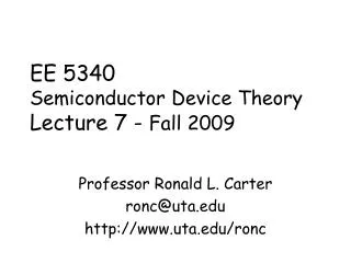
EE 5340 Semiconductor Device Theory Lecture 11 - Fall 2010. Professor Ronald L. Carter ronc@uta.edu http://www.uta.edu/ronc. E FN. Band diagram for p + -n jctn* at V a = 0. E c. qV bi = q( f n - f p ). q f p < 0. E c. E Fi. E FP. E v. E Fi. q f n > 0.

E N D
EE 5340Semiconductor Device TheoryLecture 11 - Fall 2010 Professor Ronald L. Carter ronc@uta.edu http://www.uta.edu/ronc
EFN Band diagram forp+-n jctn* at Va = 0 Ec qVbi = q(fn -fp) qfp < 0 Ec EFi EFP Ev EFi qfn > 0 *Na > Nd -> |fp|> fn Ev p-type for x<0 n-type for x>0 x -xpc xn 0 -xp xnc
Depletion approx.charge distribution r +Qn’=qNdxn +qNd [Coul/cm2] -xp x -xpc xn xnc Due to Charge neutrality Qp’ + Qn’ = 0, => Naxp = Ndxn -qNa Qp’=-qNaxp [Coul/cm2]
O O O O O O + + + - - - Induced E-fieldin the D.R. Ex N-contact p-contact p-type CNR n-type chg neutral reg Depletion region (DR) Exposed Donor ions Exposed Acceptor Ions W x -xpc -xp xn xnc 0
Soln to Poisson’sEq in the D.R. Ex xn -xp x -xpc xnc -Emax
Effect of V 0 • Define an external voltage source, Va, with the +term at the p-type contact and the -term at the n-type contact • For Va > 0, the Va induced field tends to oppose Ex due to DR • For Va < 0, the Va induced field tends to add to Ex due to DR • Will consider Va < 0 now
Band diagram forp+-n jctn* at Va 0 Ec q(Vbi-Va) q(Va) qfp < 0 Ec EFi EFN EFP Ev EFi qfn > 0 *Na > Nd -> |fp|> fn Ev p-type for x<0 n-type for x>0 x -xpc xn 0 -xp xnc
Soln to Poisson’sEq in the D.R. Ex W(Va-dV) W(Va) xn -xp x -xpc xnc -Emax(V) -Emax(V-dV)
Effect of V 0 • Lever rule, Naxp=Ndxn, still applies • Vbi = Vt ln(NaNd/ni2), still applies • W = xp +xn, still applies • Neff =NaNd/(Na +Nd), still applies • Q’n = qNdxn = -Q’p = qNaxp, still applies • For Va < 0, W increases and Emax increases
One-sided p+n or n+p jctns • If p+n, then Na >>Nd, and NaNd/(Na +Nd) = Neff --> Nd, and W --> xn, DR is all on lightly d. side • If n+p, then Nd >>Na, and NaNd/(Na +Nd) = Neff --> Na, and W --> xp, DR is all on lightly d. side • The net effect is that Neff --> N-, (- = lightly doped side) and W --> x-
Depletion Approxi-mation (Summary) • For the step junction defined by doping Na (p-type) for x < 0 and Nd, (n-type) for x > 0, the depletion width W = {2e(Vbi-Va)/qNeff}1/2, where Vbi = Vt ln{NaNd/ni2}, and Neff=NaNd/(Na+Nd). Since Naxp=Ndxn, xn = W/(1 + Nd/Na), and xp = W/(1 + Na/Nd).
n Nd 0 xn x Debye length • The DA assumes n changes from Nd to 0 discontinuously at xn, likewise, p changes from Na to 0 discontinuously at -xp. • In the region of xn, Poisson’s eq is E = r/e --> dEx/dx = q(Nd - n), and since Ex = -df/dx, we have -d2f/dx2 = q(Nd - n)/e to be solved
Debye length (cont) • Since the level EFi is a reference for equil, we set f = Vt ln(n/ni) • In the region of xn, n = ni exp(f/Vt), so d2f/dx2 = -q(Nd - ni ef/Vt), let f = fo + f’, where fo = Vt ln(Nd/ni) so Nd - ni ef/Vt = Nd[1 - ef/Vt-fo/Vt], for f - fo = f’ << fo, the DE becomes d2f’/dx2 = (q2Nd/ekT)f’, f’ << fo
Debye length (cont) • So f’= f’(xn) exp[+(x-xn)/LD]+con. and n = Nd ef’/Vt, x ~ xn, where LD is the “Debye length”
Debye length (cont) • LD estimates the transition length of a step-junction DR (concentrations Na and Nd with Neff = NaNd/(Na +Nd)). Thus, • For Va=0, & 1E13 <Na,Nd< 1E19 cm-3 • 13% <d< 28% => DA is OK
JunctionC (cont.) r +Qn’=qNdxn +qNd dQn’=qNddxn -xp x -xpc xn xnc Charge neutrality => Qp’ + Qn’ = 0, => Naxp = Ndxn -qNa dQp’=-qNadxp Qp’=-qNaxp
JunctionCapacitance • The junction has +Q’n=qNdxn (exposed donors), and (exposed acceptors) Q’p=-qNaxp = -Q’n, forming a parallel sheet charge capacitor.
JunctionC (cont.) • So this definition of the capacitance gives a parallel plate capacitor with charges dQ’n and dQ’p(=-dQ’n), separated by, L (=W), with an area A and the capacitance is then the ideal parallel plate capacitance. • Still non-linear and Q is not zero at Va=0.
JunctionC (cont.) • This Q ~ (Vbi-Va)1/2 is clearly non-linear, and Q is not zero at Va = 0. • Redefining the capacitance,
JunctionC (cont.) • The C-V relationship simplifies to
Cj-2 Cj0-2 Va Vbi JunctionC (cont.) • If one plots [Cj]-2vs. Va Slope = -[(Cj0)2Vbi]-1 vertical axis intercept = [Cj0]-2 horizontal axis intercept = Vbi