Download
1 / 16
160 likes | 297 Views
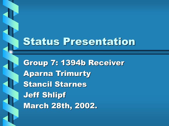
Status Presentation . Group 7: 1394b Receiver Aparna Trimurty Stancil Starnes Jeff Shlipf March 28th, 2002. Objective of presentation. To report modifications and advancements to the project since the design report. Status: stages 1 and 2 completed, stage 3 in progress. Stage 1.

E N D
Status Presentation Group 7: 1394b Receiver Aparna Trimurty Stancil Starnes Jeff Shlipf March 28th, 2002.
Objective of presentation • To report modifications and advancements to the project since the design report. • Status: stages 1 and 2 completed, stage 3 in progress
Stage 1 • Purpose: testing an optomodule out of its original environment(TI card) by placing it on a evaluation board built by the group. • Opto module used: Agilent technologies HFBR-53D5 • Status : Complete
Stage 1: Test setup • GTS 1250 GBIC test system pattern generator • Textronic TDS 7154 Digital Phosphor Oscilloscope
Ch2 K28.7 Ch 2 PRBS7 Stage 1: Test results
Stage 2 • Purpose: testing the Maxim Receiver evaluation kits • MAX 3266 – transimpedance amplifier(TIA) • MAX 3264 – limiting amplifier • Status: Complete.
Stage 2: Design details • MAX 3266 power connector design- can connect to a regular AC adaptor. • MAX 3264- changed connectors of ac adaptor to match board connector. • Caused by a lack of accurate 5V power supplies.
Stage 3 • Purpose: the design and fabrication of a functional and cost effective receiver board based on the MAXIM board • Status: in progress
Stage 3: modified design Old design New design
Stage 3: Modifications • 1.The Level pin was grounded on the 3264 to maximize output voltage. • 2.The Squelch pin was grounded on the 3264 to disable squelch. It is important to see all signals in testing, no matter how small they may be. • 3.The CAZ1 and CAZ2 pins on the 3264 are left open. In the specification sheet it is stated that for gigabit Ethernet these pins should be left open. • 4.The Filter pin was left open on the 3266 to enable DC cancellation. • 5.The Loss-of-Signal circuit was omitted to further simplify the board. This also allowed for the TH pin to be left open as this simply sets the threshold of the LOS circuit.
Stage 3: Modifications • 6.The power filtering inductors were omitted. This was possible based on the fact that three separate supplies will be used and long power cords will be used between the board and the power supplied. • 7.A single 1nF capacitor is used for decoupling the power supplies. Based on the use of three separate supplies 1nF should suffice. • 8.Decoupling capacitors for the input and output of the circuit as well as between the TIA and LA chips were left in to maintain a good signal.
Stage 3: PCB layout and design considerations • Red squares are power supplies. The input power is for the TIA, the 2 output ones are for LA ( as LA has 2 stages of amplification) • 3 separate power supplies are used to reduce noise on board. • Board layout assumes front pin of connector is ground and the inner pin is VCC. Power supplies not following this assumption will be modified to work with the design.
# Part Description Manufacturer Part Number Price (all) To Obtain 4 .01uF capacitor – 0805 ECJ-2VB1H103K $.97 Order from Digikey 3 1nF capacitor – 0805 ECU-V1H102MEN $.97 Order from Digikey 1 .1uF capacitor – 0805 ECJ-2VF1E104Z $1.06 Order from Digikey 2 100 Ohm resistors –0805 ERJ-6GEYJ101V $.80 Order from Digikey 1 67 Ohm resistor –0805 ERJ-6GEYJ680V $.80 Order from Digikey 1 50 Ohm resistor –0805 ERJ-6ENF49R9V $.90 Order from Digikey 3 SWC Power Supply Connector RAPC722 $3.12 Edgar ordered some 3 Jameco SMA connectors 901-143-6 N/a A bag in lab Proposed part list
Future Considerations • Verifying the functionality of PCB board design. • Having Bob House create the board using the gerber file • Order part list . • Work on fixing the errors in our Agilent board that are ouputing an erroneous eye. • Solder, test, and troubleshoot the new board in a similar manner as the MAXIM kits. • If board produces a good eye it should be tested in conjunction with the 1394b transmitter board and OE board.