Download
1 / 52
• 530 likes • 781 Views
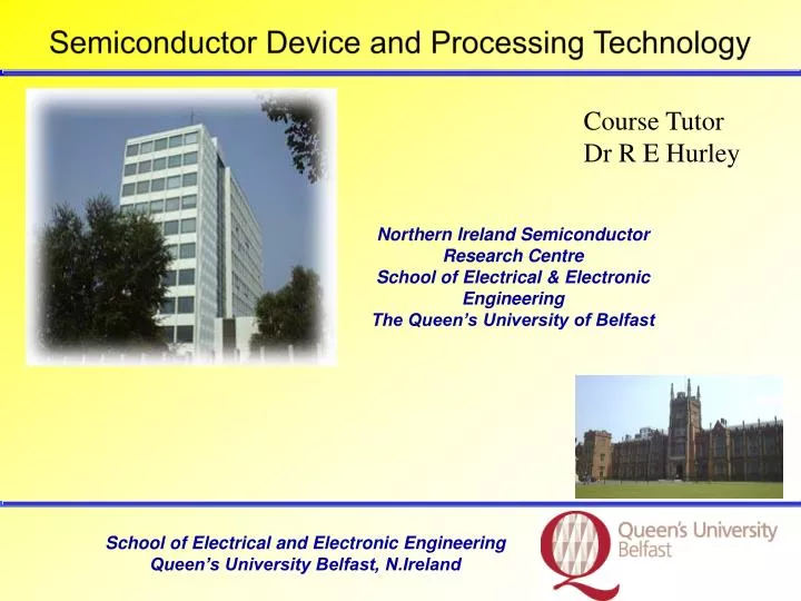
Semiconductor Device and Processing Technology. Course Tutor Dr R E Hurley. Northern Ireland Semiconductor Research Centre School of Electrical & Electronic Engineering The Queen’s University of Belfast. Semiconductor Device and Processing Technology. 7. Ion implantation History

E N D
Semiconductor Device and Processing Technology Course Tutor Dr R E Hurley Northern Ireland Semiconductor Research Centre School of Electrical & Electronic Engineering The Queen’s University of Belfast
Semiconductor Device and Processing Technology 7. Ion implantation History What’s it used for? Description and equipment Basic theory
The Basic Process +ve ion 10-200keV Crystal lattice Final destination
Early History • Goldstein’s “Kanalstrahlen” in glow discharges in 1886 • Marie Curie (alpha ray stopping) (1899) • Bohr calculated the range of heavy ions in matter, 1913 • Isotope separators developed for nuclear programme (East and West – energy and weapons, 1940s +) • Ohl (1952) First to use ions to change properties of semiconductor devices. (Improvement due to damage!?) • Lindhard, Scharff, and Schiertt (1963) • developed the theory for range and range straggling of low-energy ions. LSS used today!
Classic reference books Mayer, Eriksson, and Davies (1970) Dearnaleyet al. (1973) Wilson and Brewer (1973) Carter and Grant (1976) Ryssel and Ruge (1986) (Ion Beam, Ion Implantation Technology) conferences’ IBBM 1971a, 1971b, 1973, 1975, 1977, 1979, 1981, 1983, 1985, 1987, 1990, 1991, IIT 1981, 1982, 1985, 1987, 1989, 1991, 1993, 1995. 1993, 1995. Shockley’s 1957 ion implantation patent ( filed1954) His second invention!!
Ion implantation in the 1960s • First nuclear detectors, P+ into Si at 10 keV (Alvager and Hansen, 1962) • P-n junctions by Cs+ implantation (McCaldin and Widmer, 1963) • Chalk River Nuclear Laboratories, • Oak Ridge National Laboratory
Ion implantation in the 1960s • The Atomic Energy Research Establishment, UKAERE (Harwell) • California Institute of Technology and Stanford University (Mayer and Gibbons) • Range distributions in crystalline and amorphous semiconductors, • channeling, low-temperature and high-temperature implantation, annealing, and epitaxialrecrystallization
1969 Atomic Collisions in Solids Conference, Brighton, Mi jefe no me permitio asistir a esta conferencia (porque tenia que trabajar). ¡Pero el esperaba que yo escribiera este informe! “R E Hurley Vacuum, Volume 20, Issue 1, January 1970, Pages 15-20”
The implanter – the commercial machines 1920sMev machines for nuclear physicists (micro-amps) 1940-1945 >l000 low-energy ion separators were built in the United States to enrich Uranium 235. Each capable of 10 -100+ milli-amps!) 1946 High Voltage Engineering Corp. (HVEC) Van de Graaff and Tandem Accelerators sold to researchers. 1971 Extrion formed (Peter Rose left HVEC to form this new company). Accelerators, Inc. of Austin, Texas, (2-3 M$/year) Varian, Eltek, Eaton (1970s), Lintott
Reasons for ion implantation • Short process times • Good homogeneity and reproducibility of the profiles • Exact control of the amount of implanted ions by integrating the current. This is of particular importance for low concentrations, e.g. for adjusting the threshold voltage of MOS transistors • Relatively low temperatures during the process
Reasons for ion implantation • Different materials can be used for masking, e.g. oxide, nitride, metals, and resist Implantation through thin layers (e.g. SiO2 or Si3N4) is possible. • Low penetration depth of the implanted ions. This allows modification of thin areas near the surface with high concentration gradients. • Sequences of implantation steps (with different energies and doses) allow optimization of the dopant profiles
Disadvantages of ion implantation • Damage. Can be annealed, but where thermal budget is restricted (modern materials), can be a problem. • For very shallow profiles, enhanced diffusion and channelling limit control over depth and precise profile (as also run to run statistical variations Δx, Δy, Δz) • Channelling and its reduction by damage mean that distribution is dose dependent (P and As) For B, the damage probability is lower and the saturation of the channelling tail is not seen up to doses 5*1015 cm-2 for a conventional 70 tilt
Implantation profiles for dopants Implantation energy 100 keV
Regular distributions, little change of shape with dose Boron, mass 11 Boron, implantation energy 100 keV
Dose effect by damage • Phosphorous, mass 31 Phosphorous, implantation energy 100 keV
Dose effect by damage • Arsenic, mass 75 Arsenic, implantation energy 100 keV
Approximate symmetric Gaussian distribution Implant concentration, n(x) where the maximum concentration occurs at x = Rp, and ΔRp is the standard deviation or "straggle" of the distribution. The integral of n(x)dx gives the dose (ϕ), and the maximum concentration n(Rp ) can be written as: Rp, and ΔRp of the Gaussian distribution give a good first-order description of the implanted ions in amorphous or fine-grain polycrystalline substrates.
Energy loss = f(density of metal film). Marie Curie, 1899-1920 “Les rayons alpha sont des projectiles materielssusceptibles de perdre de leurvitesse en traversant la matiere." Marie Curie, 1899
After the Warsaw uprising Reconstruction
What are the atoms doing? Ion impact leads to cascades of recoil atoms and electrons Atomic cascades act as a nano-blender changing crystal structure and mixing atoms Electron cascades cause chemical changes (radiolysis) Foreign ion comes to rest under surface of material – ion implantation doping. Changes chemical and electronic behaviour
More precise distribution • Real distributions are skewed with long tails • An accurate analysis must distinguish: • Electronic stopping, Te (electronic excitation of target) • (For high velocity particles (electron clouds interact)) • Nuclear stopping, Tn(energy transfer to recoiling atoms). • (low velocity particles. Angular scattering occurs) • Cross-over from Te to Tndepends on atomic no. of ion • (and slightly on target)
Analysis • Energy loss/path length = - dE/dR = NS • Where N is atomic density of target, S is defined as the stopping cross-section. • S = Se + Sn = ʃ Te + ʃ Tn dσ • Where dσ(Te, Tn) is the differential cross-section depending on electronic, Te, and nuclear energy loss, Tn, per collision
Electronic Stopping Power Se(E) kSiE1/2
Analysis for MOST • Accurate analysis is complex but important for ion implantation of MOST for shallow junctions in x,y and z directions. • As ion slows down, nuclear stopping produces a long tail. Some channelling is difficult to avoid. • Monte-Carlo software programs used with corrections to allow for second-order effects. • SRIM and TRIM are available free on the web!
Stopping and Range of Ions in Matter (SRIM) • SRIM uses a Monte-Carlo program called TRIM • (Transport of Ions in Matter). • 2 main approximations • Uses Analytic formula for calculating atom-atom collisions with parameter ‘fitting’. • Uses concept ‘Free flight path between collisions,’ • to eliminate ‘non-significant’ collisions. • TRIM is widely used with a book available for serious users (and easy to use). http://www.srim.org/SRIM%20Book%20(Review%20Pages).htm
Principles of TRIM Random starting position Monte-Carlo method. Free flight path between collisions. Rate of energy loss = f(Ntarget and nuclear and electronic stopping powers)
Technique of Ion Implantation • Atoms ionised in ion source • Extracted (~ 20-30kV) • Mass separated (remove impurities) • Accelerated to high energy (20 – 300 keV) • Focused and scanned over wafer
Gas Box BF3, AsH3, PH3 Ion Source Magnet Accelerator • Target wafers
Machine requirements for semiconductors • Homogeneity (~ 2% on QUB machine over wafer) • Dose control of the implanted dopant concentration √ • scanning and current integration √ • angular control (depends on scanning system, target normally tilted at 70to avoid channelling) • Low contamination (QUB uses cryos, load-lock, rotaries?) • cooling √ • avoidance of charging √ (flood with electrons, use B field)
Electrostatic Electrostatic +Mechanical
Target scanning systems • Lintott (Harwell) chain wheel • Varian-Extrion Ferris wheel • Modern spinning disk
Contamination • Interference between doubly charged molybdenum from the ion source material and boron fluoride (11B,19F2 ~ mass 49) (Cubina and Frost, 1991). Mo = mass ~96. [ need to improve resolution!] • Direct contact between wafer and sample holder, • Non-ideal mass separation [why not?] • Charge exchange (hard to avoid) • Outgassing from implanter components. (always present) • Sputtering from internal components. (make in Si, C or Al)
Historical Trends CMOS, history • Standard metal-gate process • Self-aligned metal-gate process • Full implant of source and drain
Historical Trends CMOS, history • Self- align gate. Gate = implantation mask! = perfect registration when channels were 5-7 µm long. (Nobody knew about lateral straggle!!) • Current integration = accurate dose = control over threshold voltage and precision doping for CMOS • Al (gate) alloying with silicon meant low anneal at 550C • Later, polysilicon replaced Al as a gate material with full self-alignment..
Drain engineering for small dimension MOS devices • Impurity profile in drain region important • Hot carrier injection into gate dielectric is a problem for n-channel devices. • (3.3eV energy, electrons degrade SiO2 → leakage etc.) • Use lightly doped drain (LLD) to reduce max field in channel. (Scattering of hot electrons at drain end) • (low dose P+ implant in critical region_