Download
1 / 25
250 likes | 375 Views
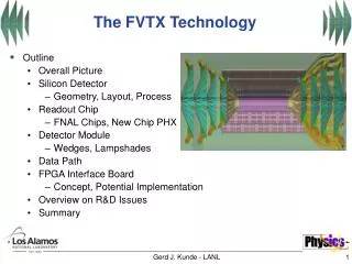
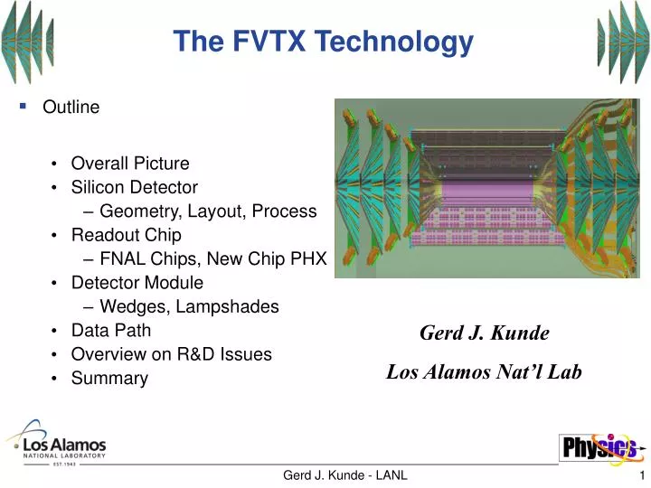
The FVTX Technology. Outline Overall Picture Silicon Detector Geometry, Layout, Process Readout Chip FNAL Chips, New Chip PHX Detector Module Wedges, Lampshades Data Path Overview on R&D Issues Summary. Gerd J. Kunde Los Alamos Nat’l Lab. FVTX Tracker Executive Summary.

E N D
The FVTX Technology • Outline • Overall Picture • Silicon Detector • Geometry, Layout, Process • Readout Chip • FNAL Chips, New Chip PHX • Detector Module • Wedges, Lampshades • Data Path • Overview on R&D Issues • Summary Gerd J. Kunde Los Alamos Nat’l Lab Gerd J. Kunde - LANL
FVTX Tracker Executive Summary • Four lampshade silicon detector stations on each side • Mini-strips with 50 micron radial pitch: 2.2 -13 mm • Readout via new PHX chip from Fermi Nat’l Lab • Total strip count: ~ 2 * 860,000 strips (zero suppressed) • Total chip count: ~ 2 * 1680 chips • Total silicon area: ~ 2 *3350 cm2 Gerd J. Kunde - LANL
The Inner Volume of PHENIX 78 cm 66 cm VTX NCC FVTX FVTX NCC 45 cm Mechanical Design for VTX and FVTX by LANL & Hytec Gerd J. Kunde - LANL
Endcap (north and south) z-start(+-) o-radius tilt = 22 deg station 1 20 cm 6.6 cm ministrip station 2 26 cm 10.6cm ministrip station 3 32 cm 18 cm ministrip station 4 38 cm 18 cm ministrip Current VTX & FVTX Specifications 1.2% 2.0% Rad. Length 1.2 % Gerd J. Kunde - LANL
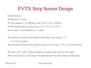
2816 2048 1280 Silicon Detector Technical Overview • 300 micron thickness • 50 micron radial pitch (z reconstruction) • curved or straight strips ? (R&D) • 1280,2048,2816 “mini-strips” • 3.5 cm < r < 18 cm • < 1.5 % occupancy (central AA) • 48 “towers” in phi • mini-strips pairs from 13.0 mm to 2.2 mm • readout via a PHX 5,8,11 chip row r = 18.0 cm r = 3.5 cm 1 PHX derived from FNAL chips Gerd J. Kunde - LANL
Only “2 ½” Silicon Detector types 50 micron strips (collaboration with Prague groups) Outside Detector (II) Outside Detector (III) Inside Detector (I) 5 chips= 1280 * 2 strips 706.2 mm^2 6 chips= 1536 * 2 strips 1698.5 mm^2 3 chips= 768 * 2 strips 752.0 mm^2 Gerd J. Kunde - LANL
Two Silicon Wafer Layout Concepts* * Discussions with vendors concerning dicing ‘p on n’ technology (much simpler than ‘n+ on n’ with moderated p-spray) Proven technology with many vendors (1st quotes are base for cost estimate) We assume 4 inch - 300 um wafers, the layout is matching the need of inner and outer detectors: Inner: 77 wafers + contingency Outer: 96 wafers + contingency Gerd J. Kunde - LANL
Construction Start Silicon Sensor Schedule Based on ON quote and BTeV/Atlas WBS Gerd J. Kunde - LANL
Existing FNAL Chip: FPIX2.1 Features • Advanced mixed analog/digital design • 128 rows x 22 columns (2816 channels) • 50 µm x 400 µm pixels • High speed readout intended for use in Level 1 trigger. Up to 840 Mbits/sec data output. • Very low noise, excellent threshold matching • DC coupled input (15 nA max leakage current per channel) • Output directly drives long cable (10 m, 30 feet) • 90 micro watt/pixel • (~0.25 watt/chip) • Rad hard to 50 Mrads Change geometry for PHX-chip and adjust analog front end to mini-strips capacitance Gerd J. Kunde - LANL
3 bit ADC PHX Simulation PHX Simulation Signal/Noise ~ 75/1 Threshold/Noise ~ 15/1 for mips ion mini-strips on 300 um Si 2 mm to 10 mm strip length FPIX 2.1 Pixel Circuit (50 x 400 µm) FPIX2: 60 e-rms measured noise @ c=0 pf Gerd J. Kunde - LANL
8 Chip Module: “Real” Threshold and Noise CHIP 4 CHIP 4 Threshold Noise ENC (e-) ENC (e-) These are typical distribution curves for threshold and noise for a FPIX 2.0 chip on an 8 chip HDI. (A mip gives ~ 24,000 electrons in 300 micron Si) Gerd J. Kunde - LANL
Measured FPIX 2.0 Power Consumption The power consumption of the 8 chip module is: for (VD=VA=2.5V) 1.86W Module idle. 2.26W Module collecting data.* 100 micro watt/channel for (VD=VA=2.2V) 1.51W Module idle. 1.83W Module collecting data.* 80 micro watt/channel * 8 chip module collecting data at 300Mbps. Gerd J. Kunde - LANL
signals & power Bump bonds Programming interface Discriminator Pipeline Digital interface signals & power FNAL Collaboration Ray Yarema’s group PHX Chip Layout: 256 channels/side 3.8 mm x 13 mm = 49.4 mm2 Thinned to 150 to 200 um Bump bonds on 200 um pitch 50 µm dia solder bumps 512 bumps plus inter-chip bumps ~ 15 wafers needed Keep all digital backend the same ! Adjust only input (keep DC coupling) and geometry, optimize the row/column structure for readout speed and add pulser. Bus on chip ? Gerd J. Kunde - LANL
PHX Bus R&D Kapton Kapton PHX PHX 300 um Silicon PHX Silicon FNAL Proposal: Power & Data Bus on Chip Bump Bonding Alternate Proposal: Power & Data Bus on Kapton Wirebonding side view Preliminary calculations by R.Yarema show that the I-R loss is acceptable, need optimize number of signal lines per chip cross section Gerd J. Kunde - LANL
FVTX Power Numbers added for both ends ! ~3400 chips, but only ~ 100 Watts per Endcap Fiber readout would require an additional 500 Watt of cooling, not directly on the detector but on the end plates Gerd J. Kunde - LANL
Construction Start PHX Chip Development Schedule Conceptual Design Chip Layout Based on R.Yarema Estimate Gerd J. Kunde - LANL
2 silicons in front 2 silicons in back Eliminate dead silicon areas by overlapping 1 mm along edges …. FVTX Wedge Assembly 3 mm carbon wedge for assembly and cooling Carbon Fiber Support and Cooling Gerd J. Kunde - LANL
From Wedges to Lampshades X 24 Total strip count: ~ 2 * 860,000 strips Total chip count: ~ 2 * 1680 chips Total silicon area: ~ 2 * 3350 cm2 Double Tower aka Wedge Gerd J. Kunde - LANL
48 per station Fiber 4 Gbit/s Serializer Optical Driver Slow Control ~100 Hz 5 x 512 channels FVTX Connections Copper Flex (Fiber) 48 per station Copper Cables 61 LVDS Pairs Copper Bus LVDS 4 x 169.8 MBit Hit: 9 bit address ,3 bit adc, 4 bit chip-id, tag 8bit => 24 bits 6 x 512 channels 5 x 512 channels • R&D Project: Flex Cables or Fiber to the ‘outside world’ ? • Space Constraints (see R.Pak) • Costs/Complexity/Reliability Gerd J. Kunde - LANL
Samtech QSS-RA100 .635mm pitch Connector (7mmx54mm) 24 Fiber MPO Connector (x8) 160 mm 30mm 12 fibers per connector FVTX Connections I ‘Collar’ board(green) and fiber optic connector(orange) • R&D Project: Flex Cables or Fibers the ‘outside world’ ? • Space Constraints (see R.Pak) Gerd J. Kunde - LANL
Copper vs. Fiber on Endplate - II • Copper: • Passive, only connectors • Radius: ~ 1 m • Fiber: • Deserializer/ Fiber drivers • Radius: ~ 0.5 m R&D issue under investigation Gerd J. Kunde - LANL
Electronics Readout ConceptAll Details in B.Cole’s Talk FVTX FEM chip download Level-1 Accept PHX Clock/Control (Serial) Bus Driver ? Data to Level-1 ~169.8 Mbits/s data push Serial Data From PHX Data to DCMs PHX chips are zero suppressed !!! Slow Control Mode Bits Clock Magnet Platform Detector Gerd J. Kunde - LANL
Serial input Parallel input Clock Counter Hit Counter Write Address Hit Counter Reset FNAL Chip/FGPA Studies at LANL • Exercising FPIX and multiple FSSR Boards (same digital backend as future PHX) • Have working deserializer & 64 ring buffer (PHENIX standard), code by S. Butsyk and A.Puwar • Features: • Zero dead time • Store up to 8 hits per beam clock • No explicit memory reset 64 x 8b Beam Clock Buffer 64 x (3b+OFL) Hit Counter 512 x 18b Dual Port Memory 8 hits 64 Beam Clocks FSSR 6 Chip Hybrid Gerd J. Kunde - LANL
FVTX Research & Development • Silicon Detector • ‘p on n’ standard strips • Straight or curved strips ? • PHX Chip • Low risk modification of existing design • Analog input, row/column structure, pulser • New development • Bus on chip or flex ? • Interfacing • Flex copper cables or Fibers • R&D • Transition Board (see B.Cole’s talk) • New development • FVTX Interface Board (FIB) and firmware • DAQ/Slow Control • Mechanics/Cooling integrated in VTX solution • See R.Pak’s presentation Gerd J. Kunde - LANL
FVTX Summary • North and South: 4 Station Precision Silicon Tracker for the Muon Arms • FNAL (BTeV) Technology for Readout Chip • Standard Silicon Strip Technology • R&D Schedule Exists (needs to start now !) • FVTX (DAQ) Interface Board with FPGA and Firmware • R &D started under LANL grant • Collaboration with Columbia/ISU • Mechanics/Infrastructure covered in talk by R.Pak • Detailed Schedule in talk by M.Brooks Gerd J. Kunde - LANL