Download
1 / 29
360 likes | 1.01k Views
Ion Implantation. ECE/ChE 4752: Microelectronics Processing Laboratory. Gary S. May March 4, 2004. Outline. Introduction Ion Distribution Ion Stopping Ion Channeling Implant Damage Annealing. Basics.

E N D
Ion Implantation ECE/ChE 4752: Microelectronics Processing Laboratory Gary S. May March 4, 2004
Outline • Introduction • Ion Distribution • Ion Stopping • Ion Channeling • Implant Damage • Annealing
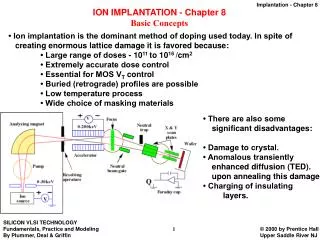
Basics • Definition: penetration of ionized dopant atoms into a substrate by accelerating the ions to very high energies • Allows precisely controlled doses of dopant atoms to be injected (1011 cm-2 to 1018 cm-2) • Used instead of pre-deposition in industry, but we don't use because of: • cost ($2M for one machine) • equipment maintenance • limited throughput • safety
Equipment Description (1) Gas source of material, such as BF3 or AsH3 at high accelerating potential; valve controls flow of gas to ion source (2) Power supply to energize the ion source (3) Ion source containing plasma with the species of interest (such as +As, +B, or +BF2), at pressures of ~ 10-3 torr (4) Analyzer magnet: allows only ions with desired charge/mass ratio through (5) Acceleration tube through which the beam passes (6) Deflection plates to which voltages are applied to scan the beam in x and y directions and give uniform implantation (7) Target chamber consisting of area-defining aperture, Faraday cage, and wafer feed mechanism
Outline • Introduction • Ion Distribution • Ion Stopping • Ion Channeling • Implant Damage • Annealing
Implanted Ions • Implantation energies typically 1 keV - 1 MeV • Ion distributions have depths of 10 nm - 10 µm • Doses vary from 1012 ions/cm2 for threshold voltage adjustment in MOSFETs to 1018 ions/cm2 for formation of buried insulating layers. • Advantages of ion implantation: (1) Precise control and reproducibility (2) Lower processing temperature
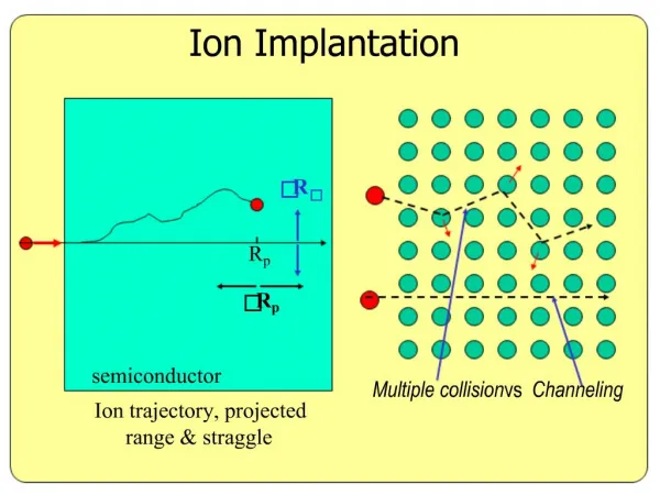
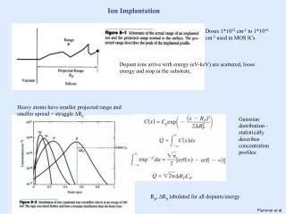
Range • Energetic ions lose energy through collisions with electrons and nuclei in substrate • Total distance an ion travels = range (R) • Projection of this distance along axis of incidence = projected range (Rp). • # collisions per unit distance and energy lost per collision are random variables; standard deviation in the projected range = projected straggle (sp) • Statistical fluctuation along an axis perpendicular to the axis of incidence = lateralstraggle (s┴)
Ion Profile • Implanted profile can be approximated by a Gaussian distribution function: where S is the ion dose per unit area • Maximum concentration is at Rp
Example For a 100 keV boron implant with a dose of 5 × 1014 cm-2, calculate peak concentration. Solution: From Fig. 6a, Rp = 0.31 mm and sp = 0.07 µm → n(Rp) = 2.85 × 1019 cm-3
Outline • Introduction • Ion Distribution • Ion Stopping • Ion Channeling • Implant Damage • Annealing
Mechanisms • Nuclear (Sn)– transfer of energy from incoming ion to target nuclei (collisions) • Ionic (Se) – interaction of incident ion with electrons surrounding target atoms (Coulombic interaction)
Stopping and Range • Average energy (E) loss per unit distance: • Total distance traveled: where: E0 = initial energy
Nuclear Stopping • When spheres collide, momentum is transferred • Deflection angle (q) and velocities, v1 and v2, can be obtained from conservation of momentum and energy • Maximum energy loss in a head-on collision:
Electronic Stopping • Proportional to velocity of incident ion: where ke is a weak function of atomic mass and number • ke ~ 107 (eV)1/2/cm for silicon
Outline • Introduction • Ion Distribution • Ion Stopping • Ion Channeling • Implant Damage • Annealing
Definition • Channeling occurs when incident ions align with crystallographic direction and are guided between rows of atoms.
Results • Only loss mechanism is electronic stopping, and range can be significantly larger than it would be in an amorphous target. • Ion channeling is particularly critical for low-energy implants and heavy ions.
Minimizing Channeling • Can be minimized by : (a) A blocking amorphous surface layer (b) Misorientation of the wafer (c) Creating a damage layer in wafer surface
Outline • Introduction • Ion Distribution • Ion Stopping • Ion Channeling • Implant Damage • Annealing
Cause of Damage • Nuclear collisions transfer energy to the lattice so that host atoms are displaced resulting in implant damage (also called lattice disorder). • Displaced atoms may in turn cause cascades of secondary displacements of nearby atoms to form a “tree of disorder” along ion path. • When displaced atoms per unit volume approach the atomic density, material becomes amorphous.
Tree of Disorder • Most energy loss for light ions (e.g., 11B+) is due to electronic collisions→ little damage, most occurs near final ion position. • For heavy ions, most energy loss is due to nuclear collisions → heavy damage.
Outline • Introduction • Ion Distribution • Ion Stopping • Ion Channeling • Implant Damage • Annealing
Basics • Process of repairing implant damage (i.e., “healing” the surface) is called annealing • Also puts dopant atoms in substitutional sites where they will be electrically active • 2 objectives of annealing: 1)healing, recrystallization(500 - 600 oC) 2) renew electrical activity (600 - 900 oC)
Boron Annealing • Annealing depends on dopant type and dose. • For a given dose, annealing temperature is temperature at which 90% of the implanted ions are activated by a 30 minute annealing in a conventional furnace. • For boron, higher annealing temperatures are needed for higher doses.
Phosphorus Annealing • At lower doses, P annealing is similar to B. • When the dose is greater than 1015 cm–2, the annealing temperature drops to about 600 °C. • At doses greater than 6 × 1014 cm–2, silicon surface becomes amorphous, and semiconductor underneath amorphous layer is a seeding area for recrystallization. • A 100 – 500 nm amorphous layer can be recrystallized in a few minutes. • Full activation can be obtained at relatively low temperatures.
Rapid Thermal Annealing • Wafer heated to 600 – 1100°C quickly under atmospheric conditions • Advantages: • Short processing time • Less dopant diffusion and contamination • Disadvantages: • Temperature measurement/control • Wafer stress and throughput