Download
1 / 49
540 likes | 987 Views
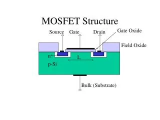
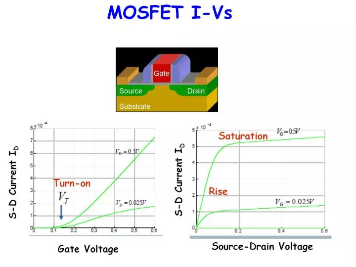
MOSFET I-Vs. V SG. V SD. More electrons. Operation of a transistor. V SG > 0 n type operation. Gate. Insulator. Source. Drain. Channel. Substrate. Positive gate bias attracts electrons into channel Channel now becomes more conductive .

E N D
MOSFET I-Vs ECE 663
VSG VSD More electrons Operation of a transistor VSG > 0 n type operation Gate Insulator Source Drain Channel Substrate Positive gate bias attracts electrons into channel Channel now becomes more conductive
Some important equations in the inversion regime (Depth direction) VT = fms + 2yB + yox yox = Qs/Cox Gate Insulator Qs = qNAWdm Source Drain Channel Wdm = [2eS(2yB)/qNA] Substrate x VT = fms + 2yB + [4eSyBqNA]/Cox Qinv = -Cox(VG - VT)
MOSFET Geometry VG Z VD L D S z y x ECE 663
How to include y-dependent potential without doing the whole problem over? ECE 663
Assume potential V(y) varies slowly along channel, so the x-dependent and y-dependent electrostats are independent (GRADUAL CHANNEL APPROXIMATION) i.e., Ignore ∂Ex/∂y Potential is separable in x and y ECE 663
How to include y-dependent potentials? VG = yS + [2eSySqNA]/Cox S = 2B + V(y) • Need VG – V(y) > VT to invert channel at y (V increases threshold) • Since V(y) largest at drain end, that • end reverts from inversion to • depletion first (Pinch off) • SATURATION [VDSAT = VG – VT] ECE 663
So current: • j = qninvv = (Qinv/tinv)v • I = jA = jZtinv = ZQinvv • Qinv= -Cox[VG – VT - V(y)] • v= -meffdV(y)/dy ECE 663
So current: • I = meffZCox[VG – VT - V(y)]dV(y)/dy Continuity implies ∫Idy = IL • I = meffZCox[(VG – VT )VD- VD2/2]/L ECE 663
But this current behaves like a parabola !! • I = meffZCox[(VG – VT )VD- VD2/2]/L ID IDsat VDsat VD We have assumed inversion in our model (ie, always above pinch-off) So we just extend the maximum current into saturation… Easy to check that above current is maximum for VDsat = VG - VT Substituting, IDsat = (CoxmeffZ/2L)(VG-VT)2 ECE 663
What’s Pinch off? 0 0 0 VD 0 VG VG 0 VG VG Now add in the drain voltage to drive a current. Initially you get an increasing current with increasing drain bias When you reach VDsat = VG – VT, inversion is disabled at the drain end (pinch-off), but the source end is still inverted The charges still flow, just that you can’t draw more current with higher drain bias, and the current saturates
Square law theory of MOSFETs NEW • I = meffZCox[(VG – VT )VD- VD2/2]/L, VD < VG - VT • I = meffZCox(VG – VT )2/2L, VD > VG - VT J = qnv n ~ Cox(VG – VT ) v ~ meffVD /L
Ideal Characteristics of n-channel enhancement mode MOSFET ECE 663
Drain current for REALLY small VD Linear operation Channel Conductance: Transconductance: ECE 663
In Saturation • Channel Conductance: • Transconductance: ECE 663
Equivalent Circuit – Low Frequency AC • Gate looks like open circuit • S-D output stage looks like current source with channel conductance ECE 663
Equivalent Circuit – Higher Frequency AC • Input stage looks like capacitances gate-to-source(gate) and gate-to-drain(overlap) • Output capacitances ignored -drain-to-source capacitance small ECE 663
Equivalent Circuit – Higher Frequency AC • Input circuit: • Input capacitance is mainly gate capacitance • Output circuit: ECE 663
Maximum Frequency (not in saturation) • Ci is capacitance per unit area and Cgate is total capacitance of the gate • F=fmax when gain=1 (iout/iin=1) ECE 663
Maximum Frequency (not in saturation) NEW (Inverse transit time) ECE 663
Switching Speed, Power Dissipation ton = CoxZLVD/ION Trade-off: If Cox too small, Cs and Cd take over and you lose control of the channel potential (e.g. saturation) (DRAIN-INDUCED BARRIER LOWERING/DIBL) If Cox increases, you want to make sure you don’t control immobile charges (parasitics) which do not contribute to current. ECE 663
Switching Speed, Power Dissipation Pdyn = ½ CoxZLVD2f Pst = IoffVD ECE 663
CMOS NOT gate (inverter) ECE 663
CMOS NOT gate (inverter) Vin = 1 Vout = 0 Positive gate turns nMOS on ECE 663
CMOS NOT gate (inverter) Vin = 0 Vout = 1 Negative gate turns pMOS on ECE 663
So what? • If we can create a NOT gate • we can create other gates • (e.g. NAND, EXOR) ECE 663
So what? Ring Oscillator ECE 663
So what? • More importantly, since one is open and one is shut at steady • state, no current except during turn-on/turn-off • Low power dissipation ECE 663
Getting the inverter output ON Gain OFF ECE 663
What’s the gain here? ECE 663
Signal Restoration ECE 663
BJT vs MOSFET NEW • RTL logic vs CMOS logic • DC Input impedance of MOSFET (at gate end) is infinite • Thus, current output can drive many inputs FANOUT • CMOS static dissipation is low!! ~ IOFFVDD • Normally BJTs have higher transconductance/current (faster!) IC = (qni2Dn/WBND)exp(qVBE/kT) ID = mCoxW(VG-VT) 2/L gm = ID/VG = ID/[(VG-VT)/2] gm = IC/VBE = IC/(kT/q) • Today’s MOSFET ID >> IC due to near ballistic operation ECE 663
What if it isn’t ideal? • If work function differences and oxide charges are present, threshold voltage is shifted just like for MOS capacitor: • If the substrate is biased wrt the Source (VBS) the threshold voltage is also shifted ECE 663
Threshold Voltage Control • Substrate Bias: ECE 663
It also affects the I-V VG The threshold voltage is increased due to the depletion region that grows at the drain end because the inversion layer shrinks there and can’t screen it any more. (Wd > Wdm) Qinv = -Cox[VG-VT(y)], I = -meffZQinvdV(y)/dy VT(y) =y+ √2esqNAy/Cox y = 2yB + V(y) ECE 663
It also affects the I-V IL = ∫meffZCox[VG – (2yB+V) - √2esqNA(2yB+V)/Cox]dV I = (ZmeffCox/L)[(VG–2yB)VD –VD2/2 -2√2esqNA{(2yB+VD)3/2-(2yB)3/2}/3Cox] ECE 663
We can approximately include this… Include an additional charge term from the depletion layer capacitance controlling V(y) Q = -Cox[VG-VT]+(Cox + Cd)V(y) where Cd = es/Wdm Q = -Cox[VG –VT - MV(y)], M = 1 + Cd/Cox ID = (ZmeffCox/L)[(VG-VT - MVD/2)VD] ECE 663
Comparison between different models Square Law Theory Bulk Charge Theory Body Coefficient Still not good below threshold or above saturation ECE 663
Mobility • Drain current model assumed constant mobility in channel • Mobility of channel less than bulk – surface scattering • Mobility depends on gate voltage – carriers in inversion channel are attracted to gate – increased surface scattering – reduced mobility ECE 663
Sub-Threshold Behavior • For gate voltage less than the threshold – weak inversion • Diffusion is dominant current mechanism (not drift) ECE 663
Sub-threshold We can approximate s with VG-VT below threshold since all voltage drops across depletion region • Sub-threshold current is exponential function of applied gate voltage • Sub-threshold current gets larger for smaller gates (L) ECE 663
Subthreshold Characteristic Subthreshold Swing ECE 663
Much of new research depends on reducing S ! • Tunneling transistor • Band filter like operation Ghosh, Rakshit, Datta (Nanoletters, 2004) (Sconf)min=2.3(kBT/e).(etox/m) Hodgkin and Huxley, J. Physiol. 116, 449 (1952a) Subthreshold slope = (60/Z) mV/decade J Appenzeller et al, PRL ‘04
Much of new research depends on reducing S ! • Increase ‘q’ by collective motion (e.g. relay) • Ghosh, Rakshit, Datta, NL ‘03 • Effectively reduce N through interactions • Salahuddin, Datta • Negative capacitance • Salahuddin, Datta • Non-thermionic switching (T-independent) • Appenzeller et al, PRL • Nonequilibrium switching • Li, Ghosh, Stan • Impact Ionization • Plummer
More complete model – sub-threshold to saturation • Must include diffusion and drift currents • Still use gradual channel approximation • Yields sub-threshold and saturation behavior for long channel MOSFETS • Exact Charge Model – numerical integration ECE 663
Exact Charge Model (Pao-Sah)– Long Channel MOSFET http://www.nsti.org/Nanotech2006/WCM2006/WCM2006-BJie.pdf ECE 663