Download
1 / 9
90 likes | 264 Views
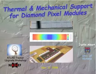
Diamond pixel VELO. To cope with higher radiation dose, LHCb might consider CVD diamond pixels for the VELO. Piggy back on ongoing developments (ATLAS, RD42, …) Polycrystyalline vs Single-Crystal CVD diamond. One possibility is to make an “all-diamond” ladder – cost compared to Silicon?

E N D
To cope with higher radiation dose, LHCb might consider CVD diamond pixels for the VELO. • Piggy back on ongoing developments (ATLAS, RD42, …) • Polycrystyalline vs Single-Crystal CVD diamond. • One possibility is to make an “all-diamond” ladder – cost compared to Silicon? • Another possibility is to just put diamond where you need the high radiation tolerance • Particle fluence reduced by ~10x in going from 1 cm3 cm (JC) • Smaller area may make single-crystal CVD diamond more viable • Exploration of “edgeless detectors” • would reduce the inactive material in active area • Would allow Si pixel and diamond pixel to be “butted” up close to one another on a single ladder. (see pages 3-4) • Some indication that can get active area ~50um from edge (see Totem NIM A paper http://dx.doi.org/10.1016/j.nima.2009.01.056) • Impact of small square frame of inactive area where Si pixel sensor and diamond sensor meet up? (see layouts on next pages)
Diamond vs Silicon ~ pCVD achieving about 10Kelectrons, saturates there…(carrier mobility saturates) scCVD signal grows with thickness(mobility doesn’t saturate up to~mm)… but only small piecesgrown so far Room temp. operation(but need cooling for electronics) LHCC-2005-003
Hybrid Si/Diamond DetectorPrecision X View Front Back
Hybrid Si/Diamond Detector Precision Y View Front Back
Edgeless detectorshttp://dx.doi.org/10.1016/j.nima.2009.01.056 (NIMA) I
Summary • We could build on RD42/ATLAS R&D on pCVD/scCVD to instrument innermost region of VELO (or entire VELO?) • Many pros for diamond.. • Rad hard, no cooling required, stable capacitance with radiation, low leakage current no thermal runaway.. • Signal at fluence~2x10¹⁶/cm2 is about 1/3 of starting value Low noise electronics • How close to edgeless can they be fabricated? • Same question for Si pixels?