Download

1 / 25
270 likes | 605 Views
ELEC1700 Computer Engineering 1 Week 8 Monday lecture Latches and flip-flops Semester 1, 2013. Revision: decoders & multiplexers Latches. Week 8. 3-to-8 decoder. binary number detected. 3-to-8 decoder. inputs. Each output corresponds to a minterm.

E N D
ELEC1700Computer Engineering 1Week 8 Monday lectureLatches and flip-flops Semester 1, 2013
Revision: decoders & multiplexers Latches Week 8
3-to-8 decoder binary number detected 3-to-8 decoder inputs Each output corresponds to a minterm • General decoders have n inputs and 2n outputs • Precisely one output asserted for each unique bit pattern • 3-to-8 decoder here (n=3) also known as: 3-line-to-8-line decoder, or 1-of-8 decoder, or 3:8 decoder
3-to-8 decoder in Logisim Week07Mon.circ – demo01
Decoder application 3-to-8 decoder • Recall: each decoder output corresponds to a minterm • To produce a sum of minterms expression, simply OR together the relevant decoder outputs!
Write out the minterm corresponding to each of the 8 outputs of a 3-to-8 decoder • Consider the truth table of a full adder below. Write Cout and S as sum of minterms • Implement a full adder with one 3-to-8 decoder and two OR gates A B Cin Cout S ------------------------------------------- 0 0 0 0 0 0 0 1 0 1 0 1 0 0 1 0 1 1 1 0 1 0 0 0 1 1 0 1 1 0 1 1 0 1 0 1 1 1 1 1 Week07Mon.circ – demo03
The truth table below describes a 74138 3-to-8 decoder • What conditions are needed to enable the decoder? • Implement a full adder with one 74138 decoder and two gates
D0 Y D1 4-to-1 MUX D2 D3 S1 S0 Multiplexer (MUX) Data input selected by S1S0 is directed to output Y S1S0= 00 : Y = D0 S1S0 = 01 : Y = D1 S1S0 = 10 : Y = D2 S1S0 = 11 : Y = D3 • Write the Boolean expression for the output Y of the 4-to-1 MUX • Write the truth table for a 4-to-1 MUX
MUX application D0 D1 D2 Y 8-to-1 MUX D3 D4 A D5 B D6 C D7 Use a 74151 8-to-1 MUX to implement the Boolean function in the truth table below A2 A1 A0 Y -------------------------- 0 0 0 1 0 0 1 1 0 1 0 0 0 1 1 1 1 0 0 0 1 0 1 0 1 1 0 1 1 1 1 1 A2A1A0
Revision: decoders & multiplexers Latches Week 8
The story so far • All logic circuits in ELEC1700 so far share one common feature: output(s) depends only on the present input(s) • Circuits so far have no storage or memory • We call these combinationallogic circuits • Example: we know how to add two numbers. But, so far: • we have no way of adding two numbers, then adding a third (a sequential operation) • we have no way of remembering or storing information after inputs have been removed • We need sequential logic circuits capable of storing intermediate results
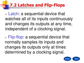
SET-RESET (S-R) latches • A latch is a type of memory device with two stable states • called a bistable logic device • Formed with cross-coupled NOR or NAND gates • Characteristic feature of all latches and flip-flops is FEEDBACK
– – Stable states of latch A B (A·B)’ 0 0 1 0 1 1 1 0 1 1 1 0 Assume both S’ and R’ inputs are HIGH 1 0 0 1 1 0 0 1 RESET state when Q=0 SET state when Q=1 In normal operation: latch outputs Q and Q’ are complements of each other
1 1 RESET pulse SET pulse – 0 0 latch in Logisim Week08Mon_NANDlatch.circ
SET RESET No change Invalid
– Truth table and symbol for latch Invalid because next state of latch cannot be reliably predicted Depends on propagation delays of the negative-OR gates
– Timing diagram for latch Sketch the latch output Q for the SET/RESET signals shown Output Q is initially LOW
Latch application: switch debouncing • Mechanical switch contacts “bounce” • Physically vibrate before making solid contact • Voltage spikes unacceptable in digital systems • Switch normally at 1 and latch RESET • Switch to 2 takes LOW (and HIGH) → SETs latch • Further voltage spikes on do not affect latch output Lab #2 uses latch for switch debouncing
Gated S-R latch • Latch will not change state until enable (EN) is HIGH • As long as EN is HIGH, latch output is controlled by S and R • Invalid state still occurs when S and R both HIGH (when enabled)
Gated S-R latch in Logisim Week08Mon_gatedSRlatch.circ
Gated S-R latch timing diagram Sketch the gated S-R latch output Q for the SET/RESET and enable (EN) signals shown Output Q is initially LOW
Q Q Gated D latch D Q D Q EN EN No invalid state, since S and R inputs in gated S-R latch can never be HIGH at the same time • D = data • Builds on S-R latch • Q follows D when enable is asserted
Gated D latch in Logisim Week08Mon_gatedDlatch.circ
Gated D latch timing diagram Sketch the gated D latch output Q for the DATA (D) and enable (EN) signals shown Output Q is initially LOW
From latches to flip-flops • Like latches, flip-flops are also bistable devices • But the output of a flip-flop only changes at a specified time • “triggering” time is specified by a clock signal • either rising edge ↑or falling edge ↓ of clock • Next week: we look at… • flip-flops • state machines built from flip-flops