Download
1 / 37
380 likes | 658 Views
EE534 VLSI Design System Summer 2004 Lecture 10:Chapter 7 CMOS Equivalent inverter and layout. Review: Construction of PDN. NMOS devices in series implement a NAND function NMOS devices in parallel implement a NOR function. A • B. A. B. A + B. A. B. Review: CMOS NAND. A. B.

E N D
EE534VLSI Design SystemSummer 2004 Lecture 10:Chapter 7 CMOS Equivalent inverter and layout
Review: Construction of PDN • NMOS devices in series implement a NAND function • NMOS devices in parallel implement a NOR function A • B A B A + B A B
Review: CMOS NAND A B A • B A B A B
weaker PUN • The threshold voltage of M2 is higher than M1 due to the body effect () VTn1 = VTn0 VTn2 = VTn0 + ((|2F| + Vint) - |2F|) since VSB of M2 is not zero (when VB = 0) due to the presence of Cint Review: VTC is Data-Dependent 0.5/0.25 NMOS 0.75 /0.25 PMOS A B M3 M4 F= A • B D A M2 S VGS2 = VA –VDS1 D Cint B M1 S VGS1 = VB
Rp Rp B A Cint CL Rn B Input Pattern Effects on Delay-I • Delay is dependent on the pattern of inputs • Low to high transition • both inputs go low • delay is 0.69 Rp/2 CL since two p-resistors are on in parallel • one input goes low • delay is 0.69 Rp CL • High to low transition • both inputs go high • delay is 0.69 2Rn CL • Adding transistors in series (without sizing) slows down the circuit Rn A
Delay Dependence on Input Patterns-II The reason for difference in low to high transition is due to internal node capacitance and high to low is Due to initial state of the internal nodes. 2-input NAND with NMOS = 0.5m/0.25 m PMOS = 0.75m/0.25 m CL = 10 fF A=B=10 A=1 0, B=1 Voltage, V A=1, B=10 time, psec Conclusions:Estimates of delay can be fairly complex – have to consider internal node capacitances and the data patterns
CMOS gate design • Designing a CMOS gate: • Find pulldown NMOS network from logic function or by inspection • Find pullup PMOS network • By inspection • Using logic function • Using dual network approach • Size transistors using equivalent inverter • Find worst-case pullup and pulldown paths • Size to meet rise/fall or threshold requirements
Equivalent inverter: effective width to length ratios (model I) Parallel combination Series combination For the NAND gate the effective length of the driver transistors doubles. That means the effective aspect ratio is decreased. . For the NOR gate the effective width of the drivers transistors doubles. That means the effective aspect ratio is increased.
Exercise: Design and compare two input NAND and NOR gates • Find W/L relationship between NMOS and PMOS transistors • Assume K'n=2K'p NAND gate NOR gate
Analysis of CMOS gates • Represent “on” transistors as resistors 1 1 W R W R 1 W R • Transistors in series → resistances in series • Effective resistance = 2R • Effective width = ½ W
Analysis of CMOS gates, cont • Represent “on” transistors as resistors R R W W W R 0 0 0 • Transistors in parallel → resistances in parallel • Effective resistance = ½ R • Effective width = 2W
Equivalent Inverter • CMOS gates: many paths to Vcc and Gnd • Multiple values for VTH, VIL, VOL, etc • Different delays for each input combination • Equivalent inverter • Represent each gate as an inverter with appropriate device width • Include only transistors which are on or switching • Calculate VTH, delays, etc using inverter equations
Static CMOS Logic Characteristics • For VTH, the VTH of the equivalent inverter is used (assumes all inputs are tied together) • For specific input patterns, VTH will be different • For VIL and VIH, only the worst case is interesting since circuits must be designed for worst-case noise margin • For delays, both the maximum and minimum must be accounted for in race analysis
Equivalent Inverter: VTH • Example: NAND gate threshold VTHThree possibilities: • A & B switch together • A switches alone • B switches alone • What is equivalent inverter for each case?
CMOS NAND gate and its inverter equivalent • Can we estimate switching threshold of the NAND gate by using CMOS inverter expression for the switching threshold? If Kn=Kp, Vth=? WP WP 2WP 2KP WN ½ WN Kn/2 WN
Equivalent inverter: Worse case delay design consideration • Represent complex gate as inverter for delay estimation • Use worse-case delays • Example: NAND gate • Worse-case (slowest) pull-up: only 1 PMOS “on” • Pull-down: both NMOS “on” WP WP WP KP WN ½ WN Kn/2 WN
CMOS NOR gate: design consideration One input Two input For N inputs
Equivalent inverter • Problems with equivalent inverter method: • Need to take into account load capacitance CL • Depends on number of transistors connected to output (junction capacitances) • Even transistors which are off (not included in equivalent inverter) contribute to capacitance • Need to include capacitance in intermediate stack nodes. Worse-case: need to charge/discharge all nodes • Body effect of stacked transistors
Transistor Sizing NAND gate NOR gate
Transistor sizing: an approach • If MOSFET serially connected in a current path, the overall current path resistance will be • All serially connected MOSFET can be replace with a single MOSFET as If the MOSFET are connected in parallel combination then,
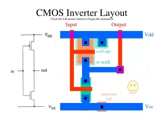
VDD tub ties transistors GND Review: Inverter layout + (Wells not shown) out a a out
VDD well ties GND NAND layout + out out b a b a
NOR gate + b a out
VDD tub ties GND NOR layout b a b out out a
4-input NAND Gate Vdd Out GND In1 In2 In3 In4
Graph-based dual network • Draw network for PUN or PDN • Circuit nodes are vertexes • Transistors are edges F F A B A B gnd
Graph-based dual network (2) • To derive dual network: • Create new node in each enclosed region of graph • Draw new edge intersecting each original edge • Edge is controlled by inverted input A B A B B A F
V V DD DD Stick Diagrams Contains no dimensions Represents relative positions of transistors Inverter NAND2 Out Out In A B GND GND
X PUN C i VDD X B A j PDN GND Dual Graph concept Logic Graph A j C B X = C • (A + B) C i A B A B C
CMOS gate layout • Goal: minimum area • Method • Minimize diffusion breaks (reduces capacitance on internal nodes) • Align transistors with common gates above each other in layout (minimizes poly length) • Group PMOS and NMOS transistors together • Approach: • Use Euler path method to find ordering of transistors in layout
Layout: Euler path method • Goal: layout without diffusion breaks • Method for finding ordering of transistors in layout → Euler path • Euler path → path through a graph that traverses each edge only once • Find common Euler path in pullup and pulldown graph • This gives the ordering of inputs in the layout
Layout: Euler path method C E B A C E D Vcc D A B F F A C Gnd E B D • Order transistors gates according to Euler path • Connect Vcc and Gnd • Make other connections according to circuit diagram Euler path: B→A→C→E→D